Deposit removing method and substrate processing method

a technology of deposit removal and substrate, which is applied in the direction of cleaning process and apparatus, cleaning of hollow articles, chemistry apparatus and processes, etc., can solve the problems of difficult to remove the cn-type reaction product, difficult to stably produce plasma, and difficult to stably produce electric fields, etc., to achieve the effect of reliable removal of the deposit produced

Inactive Publication Date: 2009-08-20
TOKYO ELECTRON LTD
View PDF7 Cites 7 Cited by
  • Summary
  • Abstract
  • Description
  • Claims
  • Application Information

AI Technical Summary

Benefits of technology

[0011]The present invention provides a deposit removing method and a substrate processing method that can reliably remo

Problems solved by technology

If deposit becomes attached to the showerhead, it becomes difficult to stably produce an electric field in the processing chamber, and therefore, plasma cannot be st

Method used


Image

  • Deposit removing method and substrate processing method
  • Deposit removing method and substrate processing method
  • Deposit removing method and substrate processing method

Examples


Embodiment Construction

[0030]The present invention will now be described in detail with reference to the drawings showing a preferred embodiment thereof.

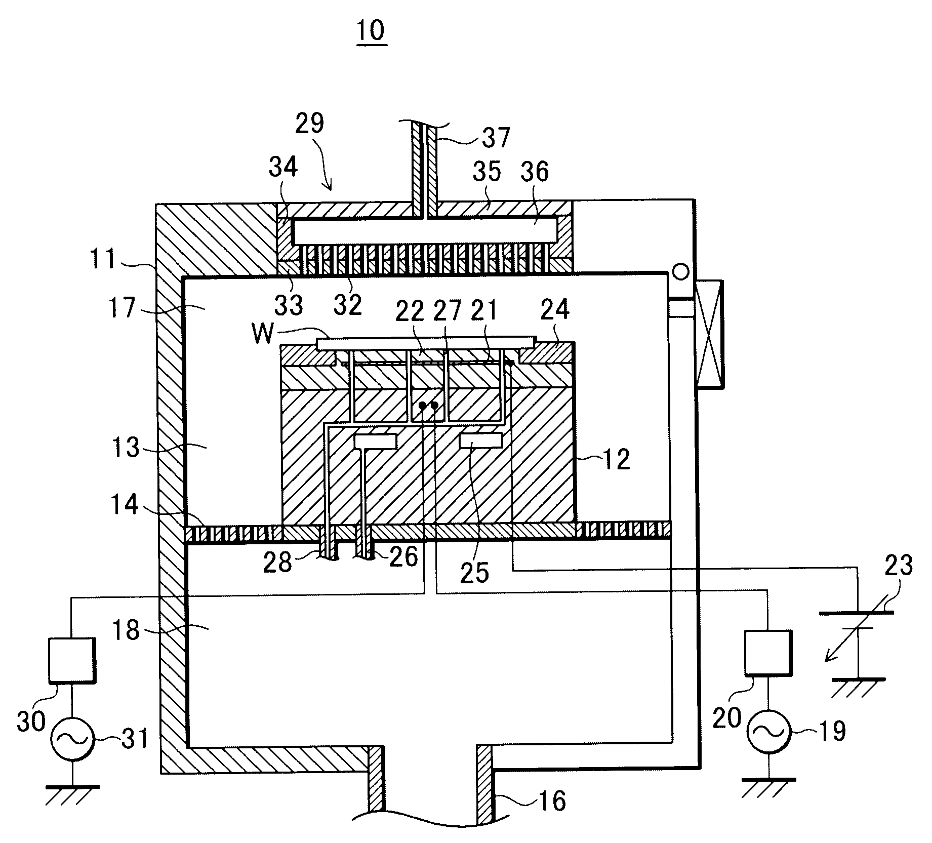
[0031]FIG. 1 is a cross-sectional view schematically showing the construction of a substrate processing apparatus that executes a deposit removing method according to the present embodiment. The substrate processing apparatus is constructed such as to carry out plasma etching processing on a semiconductor wafer as a substrate.

[0032]Referring to FIG. 1, the substrate processing apparatus 10 has a chamber 11 (processing chamber) in which a semiconductor wafer (hereinafter referred to merely as a “wafer”) W having a diameter of, for example, 300 mm is accommodated, and a cylindrical susceptor 12 on which the wafer W is mounted is disposed in the chamber 11. Moreover, in the substrate processing apparatus 10, an exhaust flow path 13 that acts as a flow path through which gas above the susceptor 12 is exhausted out of the chamber 11 is formed between the inner...


PUM

PropertyMeasurementUnit
Pressureaaaaaaaaaa
Poweraaaaaaaaaa
Poweraaaaaaaaaa

Abstract

A deposit removing method that can reliably remove deposit produced in plasma processing using plasma produced from a process gas containing methane gas and oxygen gas. In a chamber in which an electrode to which radio frequency electrical power is supplied is disposed, plasma processing is carried out on a substrate using the plasma produced from the process gas containing methane gas and oxygen gas, and then a cleaning step is carried out in which plasma is produced from a mixed gas containing fluorinated compound gas containing hydrogen in the chamber.

Description

BACKGROUND OF THE INVENTION[0001]1. Field of the Invention[0002]The present invention relates to a deposit removing method and a substrate processing method, and in particular relates to a deposit removing method in which deposit resulting from plasma produced from a process gas containing methane gas and nitrogen gas.[0003]2. Description of the Related Art[0004]In general, plasma etching processing in which trenches, holes, and so on are formed in a semiconductor wafer is carried out in an evacuated processing chamber in which a semiconductor wafer is accommodated. In the processing chamber, a mounting stage on which the semiconductor wafer is mounted, and a showerhead that supplies a process gas into the processing chamber are disposed. The mounting stage is connected to a radio frequency power source and acts as an electrode that applies radio frequency voltage to the interior of the processing chamber. The mounting stage produces an electric field in the processing chamber, and ...

Claims


Application Information

Patent Timeline
IPC IPC(8): B08B6/00
CPCH01L21/67069
Inventor LEE, SUNGTAENAKAGAWA, YUSUKEYASHIRO, JUN
Owner TOKYO ELECTRON LTD
Why Eureka
Try Eureka