Pattern inspection method and inspection apparatus

a technology of inspection apparatus and pattern, which is applied in the direction of material analysis using wave/particle radiation, instruments, nuclear engineering, etc., can solve the problems of further decrement of throughput when compared with optical systems, inability to obtain inability to achieve the adequate contrast of target regions, etc., to achieve high precision, defect detection, and high precision

Inactive Publication Date: 2009-08-20
HITACHI HIGH-TECH CORP
View PDF8 Cites 18 Cited by
  • Summary
  • Abstract
  • Description
  • Claims
  • Application Information

AI Technical Summary

Benefits of technology

[0011]The present invention has been developed in view of the above problems and an object thereof is to detect defects that are difficult to detect from an optical image with high precision by using an electron beam image and at the same time, to prevent throughput degradation of an inspection apparatus and an inspection method caused during detection as much as possible.
[0012]The present invention also provides an inspection apparatus and an inspection method excellent in that high-sensitivity defect detection performance is achieved without causing throughput degradation even if an adequate contrast of a defective region cannot be obtained due to characteristics of a wafer.
[0014]That is, a pattern inspection apparatus according to the present invention is an inspection apparatus for detecting defects of a sample and includes a scanning means for causing an electron beam to repeatedly scan the sample reciprocatingly on a line, an image acquisition means for generating an image based on secondary electrons or reflected electrons generated from the sample, a defect detection means for detecting defects from an image generated by the image acquisition means, a control means for controlling a scan with an electron beam by the scanning means, and a setting means for setting scanning conditions for the electron beam controlled by the control means, wherein the setting means has a means for setting an operation by a forward scan of the electron beam to any one of image acquisition, precharging, and discharging. A pattern inspection method according to the present invention is a method by which defective portions are determined from an image generated based on secondary electrons or reflected electrons generated from a sample after causing an electron beam to repeatedly scan the sample reciprocatingly on a line, wherein an image is acquired by a forward scan of the electron beam and an image, precharging, or discharging is acquired by a backward scan of the electron beam. Accordingly, the inspection method can be set to an optimal one depending on nature of the inspected sample so that defects on the surface of the inspected sample can be detected with high precision.
[0015]In the pattern inspection apparatus in another aspect of the present invention, the setting means has a means for setting a scanline of a forward scan and that of a backward scan by the electron beam caused to scan by the scanning means. Particularly, the setting means has a means for making settings so that after an L-th (L is a natural number) line being scanned by a forward scan of the electron beam, an (L−M)-th line (M is a natural number smaller than L) is scanned by a backward scan and further, a means for making settings so that after the (L−M)-th line being scanned by the backward scan, an (L+N)-th (N is a natural number) line is scanned by a forward scan. Similarly, in the pattern inspection method of the present invention, when the electron beam is caused to repeatedly scan reciprocatingly on a line, a scanline of the forward scan and that of the backward scan are each controlled. Particularly, after an L-th (L is a natural number) line being scanned by a forward scan of the electron beam, control is exerted so as to scan an (L−M)-th line (M is a natural number smaller than L) by a backward scan and further, after the (L−M)-th line being scanned by the backward scan, control is exerted so as to scan an (L+N)-th (N is a natural number) line by a forward scan. Accordingly, a time interval can be provided between a forward scan and a backward (retrace) scan so that defect detection with higher precision can be achieved by making a defective portion clearer. Moreover, throughput degradation is not caused because the backward scan is used effectively.
[0016]In the pattern inspection apparatus in another aspect of the present invention, the setting means has a means for making settings so that after an L-th (L is a natural number) line being scanned by a forward scan of the electron beam, an (L+M)-th line (M is a natural number) is scanned by a backward scan and further, a means for making settings so that after the (L+M)-th line being scanned by the backward scan, an (L−N)-th (N is a natural number smaller than L) line is scanned by a forward scan. Similarly, in the pattern inspection method, after an L-th (L is a natural number) line being scanned by a forward scan of the electron beam, control is exerted so as to scan an (L+M)-th line (M is a natural number) by a backward scan and further, after the (L+M)-th line being scanned by the backward scan, control is exerted so as to scan an (L−N)-th (N is a natural number smaller than L) line by a forward scan. Accordingly, a time interval can be provided between a forward scan and a backward scan so that defect detection with higher precision can be achieved by making a defective portion clearer. Moreover, throughput degradation is not caused because the backward scan is used effectively.
[0018]Further, in the pattern inspection apparatus of the present invention, the setting means may be a GUI (Graphical User Interface) to which a user can set the scanning method and conditions from outside. Similarly, in the pattern inspection method, instructions concerning the scanning method of an electron beam may be made to be entered through the GUI. Accordingly, the user can easily select the optimal scanning method and conditions depending on characteristics of an inspected sample with excellent visibility and operability.

Problems solved by technology

One problem is that because each line is scanned with an electron beam in an unicursal fashion in the SEM system, one pixel is detected as a time and thus, throughput degrades when compared with an optical system in which a line can be captured at a time.
Further, with one-time electron beam irradiation with a single stroke, the contrast of an image may vary or an adequate contrast of a target region may not be obtained, depending on characteristics of wafer.
In such a case, as described in Japanese Unexamined Patent Application Publication No. 2005-17533A, the dose of an electron beam is increased by irradiating the same line with an electron beam a plurality of times. According to this method, however, throughput described above further degrades, presenting a serious problem.

Method used


Image

  • Pattern inspection method and inspection apparatus
  • Pattern inspection method and inspection apparatus
  • Pattern inspection method and inspection apparatus

Examples


first embodiment

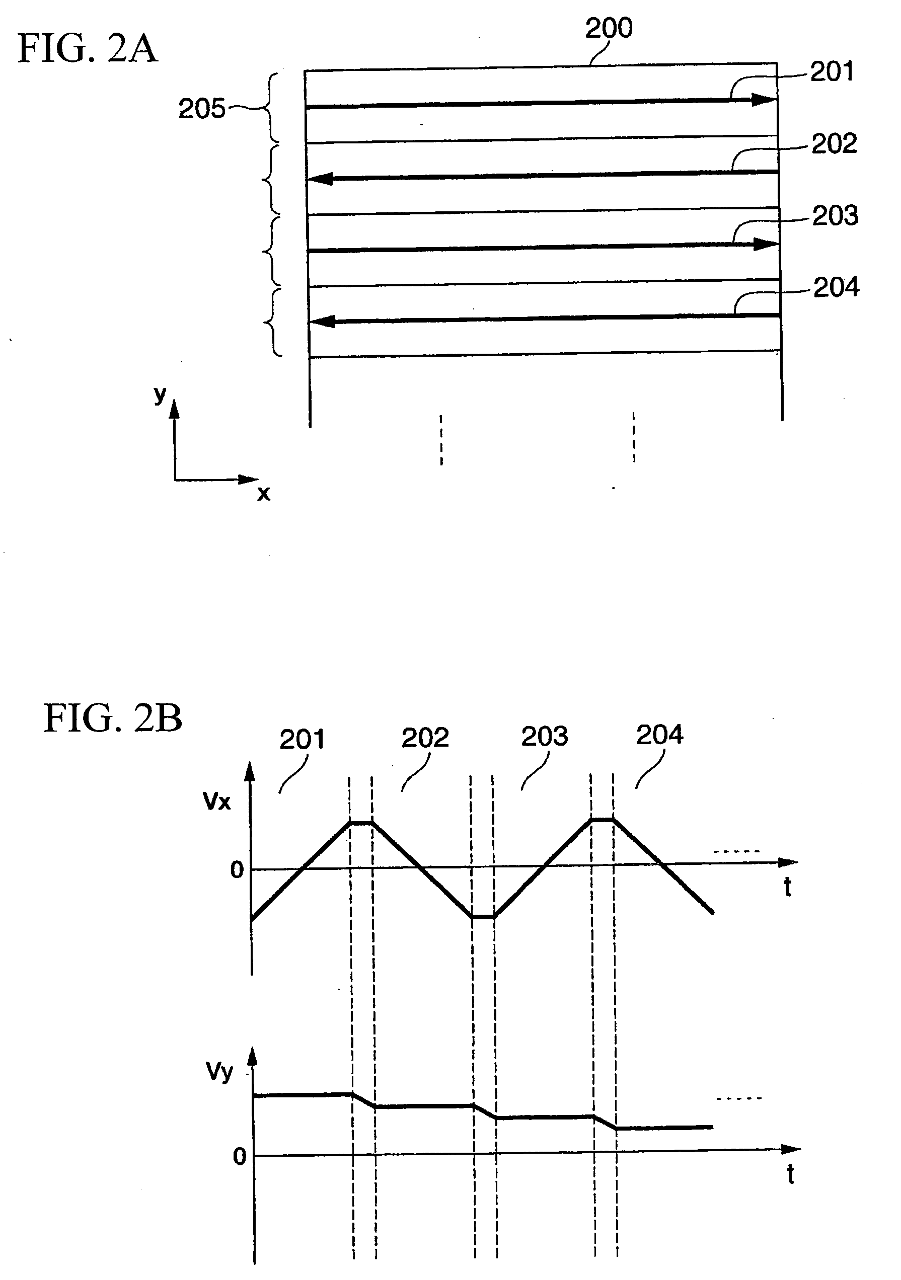
[0053]FIG. 2A and FIG. 2B are diagrams showing the first embodiment regarding the operation of the SEM pattern inspection apparatus 1 of the present invention. FIG. 2A shows how an inspection stripe 200 being scanned for each line pitch 205 in turn from above. FIG. 2B shows deflection voltages Vx and Vy of the scanning deflector 15 during scanning (In this case, it is assumed that the scanning deflector 15 uses an electrostatic deflection system).

[0054]In the present invention, the electron beam 19 can be controlled for scanning in both directions (forward and backward) by the control part 6, the correction control circuit 43, and the scanning signal generator 44. This means that, as shown in FIG. 2B, the scanning deflector 15 is capable of outputting a ramp waveform with high precision, in which the deflection voltage Vx in the principal direction (the x direction in this case) shows an upward slant to the right and a downward slant to the right. Accordingly, as shown in FIG. 2A, s...

second embodiment

[0058]FIG. 3A and FIG. 3B are diagrams showing the second embodiment regarding the operation of the SEM pattern inspection apparatus 1 of the present invention. FIG. 3A and FIG. 3B show an example in which the line 205 is precharged by using a scan from right to left (for example, reference numeral 211) corresponding to a retrace (backward scan) before an inspection scan 212 is performed. The scan 211 and the scan 212 are drawn in FIG. 3A by shifting from each other, but this is intended only to make the figure more legible and does not necessarily apply. That is, scans may actually be performed as if to follow exactly the same place within the line 205 (This also applies to figures below). In contrast to FIG. 2A and FIG. 2B, reference numerals 211, 213, 215, and 217 (broken lines) only shine an electron beam and do not acquire inspection image data.

[0059]By adopting the scanning mode described above, there is no need to reverse the order of image data in backward scans as described...

third embodiment

[0061]FIG. 4A and FIG. 4B are diagrams showing the third embodiment regarding the operation of the SEM pattern inspection apparatus 1 of the present invention. FIG. 4A and FIG. 4B show, in contrast to FIG. 3A and FIG. 3B, an example in which increased charges applied by an inspection scan are discharged by a retrace scan of reference numeral 222 on the same line 205 (performing a backward scan) after an inspection scan 221.

[0062]Like FIG. 3A and FIG. 3B, no inspection image data is acquired in the backward scans and thus, there is no need to reverse the order of data. Depending on the inspection sample or scanning environment, increased charges by an inspection scan may adversely affect defect detection of the next line and even in such a case, according to the present embodiment, discharging can be achieved while throughput degradation being minimized, so that the defect detection ratio can be increased.


PUM

PropertyMeasurementUnit
energyaaaaaaaaaa
defectsaaaaaaaaaa
defect detectionaaaaaaaaaa

Abstract

An object of the present invention is to provide an inspection apparatus and an inspection method excellent in that high-sensitivity defect detection performance is achieved without causing throughput degradation even if an adequate contrast of a defective region cannot be obtained due to characteristics of an inspected sample. To achieve the object, according to the present invention, an SEM pattern inspection apparatus for determining defective portions from an image generated based on secondary electrons or reflected electrons generated from the sample after causing an electron beam to repeatedly scan the inspected sample reciprocatingly on a line has a function to use a retrace of the electron beam for image acquisition, precharging, or discharging.

Description

BACKGROUND OF THE INVENTION[0001]1. Field of the Invention[0002]The present invention relates to an inspection apparatus and an inspection method for inspecting semiconductor devices, substrates, photo masks (masks for exposure), liquid crystals and the like having fine patterns using a scanning electron microscope.[0003]2. Description of the Related Art[0004]A semiconductor device such as a memory and microcomputer used in a computer and like is manufactured by repeating a process of transferring patterns such as circuits formed on a photo mask by exposure processing, lithography processing, etching processing or the like. Quality of results of lithography processing, etching processing and other processing and presence of defects such as foreign matter generation in manufacturing processes of semiconductor devices significantly affect manufacturing yields of semiconductor devices. Therefore, in order to detect an occurrence of abnormal conditions or failures at an early stage or i...

Claims


Application Information

Patent Timeline
Patent Type & Authority Applications(United States)
IPC IPC(8): G01N23/00
CPCH01J2237/2817H01J37/28
Inventor GUNJI, YASUHIRONINOMIYA, TAKU
Owner HITACHI HIGH-TECH CORP
Why Eureka
Try Eureka