Package structure of compound semiconductor device and fabricating method thereof

Inactive Publication Date: 2009-08-20
ADVANCED OPTOELECTRONICS TECH
View PDF4 Cites 27 Cited by
  • Summary
  • Abstract
  • Description
  • Claims
  • Application Information

AI Technical Summary

Benefits of technology

[0009]One aspect of the present invention provides the package structure of a compound semiconductor device and fabricating method thereof. The semiconductor device has external electrodes or contacts

Problems solved by technology

However, the current trend of consumer electronic products is toward lightweight, small packages.
On the other hand, the insulation layer 13c is made mostly of epoxy resin with poor heat dissipation, and ther

Method used


Image

  • Package structure of compound semiconductor device and fabricating method thereof
  • Package structure of compound semiconductor device and fabricating method thereof
  • Package structure of compound semiconductor device and fabricating method thereof

Examples


Embodiment Construction

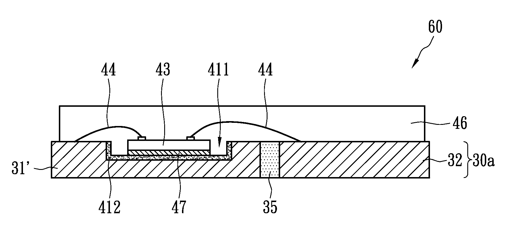
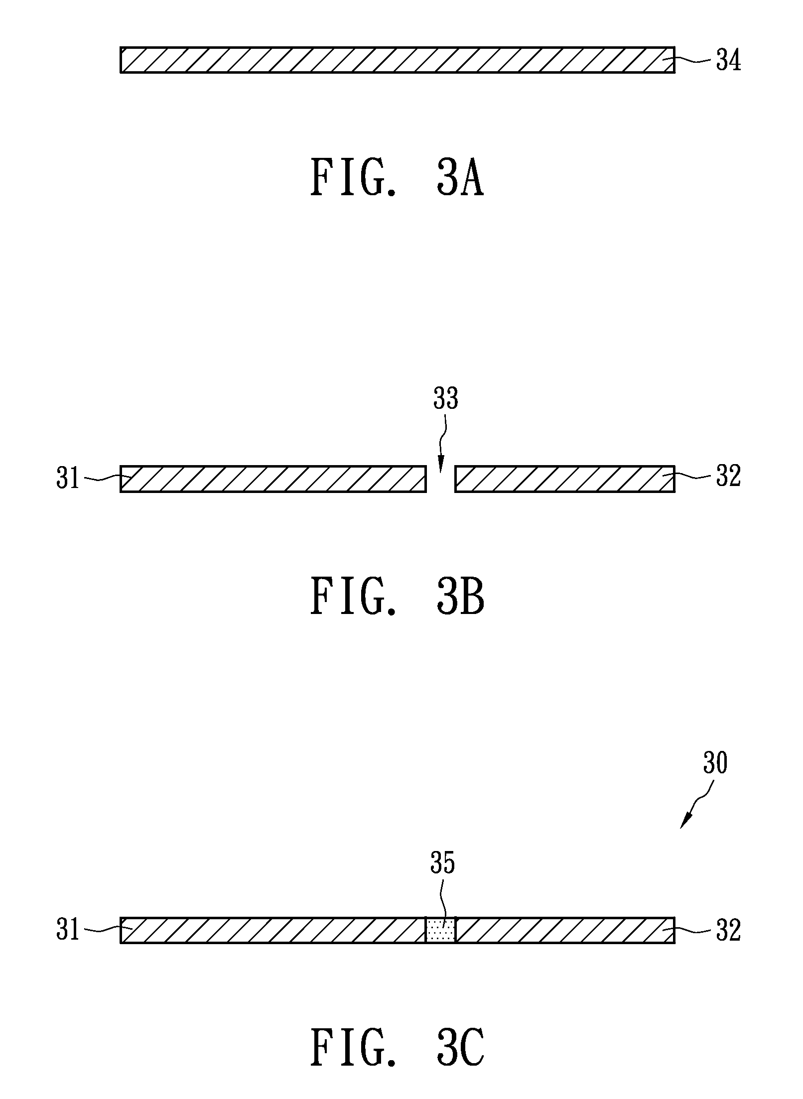
[0037]FIGS. 3A-3C are schematic illustrations showing the manufacturing steps of a thin film substrate in accordance with the present invention. As shown in FIG. 3A, a sheet 34 with a thickness of between 20-50 μm is provided; for instance copper foil or a metal film with superior conductivity. Moreover, a slot 33 is formed on the sheet 34 by a drilling process, an etching process or a punching process. The slot 33 separates a first conductive film 31 at one side from a second conductive film 32 at another side, that is, they are electrically isolated from each other, as shown in FIG. 3B. Subsequently, an insulating dielectric material 35 is filled in the slot 33 so that the manufacture of a thin film substrate 30 is finished. The insulating dielectric material 35 can be SiO, SiN, SiON, TaO, AlO, TiO, AlN, TiN, epoxy resin, silicone or polymer. In this regard, the electrical insulation between the first conductive film 31 and second conductive film 32 is improved, and the thin film ...


PUM


Abstract

A package structure of a compound semiconductor device comprises a thin film substrate, a die, at least one metal wire and a transparent encapsulation material. The thin film substrate comprises a first conductive film, a second conductive film, and an insulating dielectric material. The die is mounted on the surface of the first conductive film, and is electrically connected to the first conductive film and the second conductive film through the metal wire. The transparent encapsulation material overlays the first conductive film, second conductive film, and die. The surfaces of the first conductive film and second conductive film which is opposite the transparent encapsulation material act as electrodes. The insulating dielectric material is between the first conductive film and second conductive film.

Description

BACKGROUND OF THE INVENTION[0001](A) Field of the Invention[0002]The present invention relates to a package structure of a compound semiconductor device and fabricating method thereof, and more particularly, to a thin package structure and fabricating method of a photoelectric semiconductor device.[0003](B) Description of the Related Art[0004]Because the light emitting diode (LED) pertaining to the photoelectric device has advantages of a small body, high efficiency and long life, it is expected to be an excellent illumination source into the next generation. In addition, LCD (liquid crystal display) technology is developing rapidly and full color is the current trend in electronic product displays. Therefore, white series LEDs are not only applicable to indication lights and large size display screens but also to most consumer electronic products such as mobile phones and personal digital assistants (PDA).[0005]FIG. 1 is a schematic cross sectional diagram of the conventional SMD (...

Claims


Application Information

Patent Timeline
IPC IPC(8): H01L33/00H01L21/50H01L33/48
CPCH01L31/0203H01L33/486H01L2224/48247H01L2224/32245H01L2224/16245H01L24/45H01L2224/32257H01L2224/45144H01L2224/73265H01L2224/48091H01L2924/00014H01L2924/00H01L2924/12042H01L2924/12041H01L2924/12043H01L2224/05573H01L2224/05568H01L2924/181H01L2224/05553H01L24/05H01L2224/05599H01L2924/00012
Inventor CHEN, PIN CHUANLIN, SHEN BO
Owner ADVANCED OPTOELECTRONICS TECH
Why Eureka
Try Eureka