Nitride semiconductor device and power conversion apparatus including the same

a technology of nitride semiconductor and power conversion apparatus, which is applied in the direction of semiconductor devices, semiconductor/solid-state device details, electrical apparatus, etc., can solve the problems of increasing the power consumption of transistors, affecting the efficiency of nitride semiconductor transistors, and difficult to provide nitride semiconductor transistors with low electric loss in off-action for high-power applications, so as to achieve less electric loss, less leakage current, and less electric loss

Inactive Publication Date: 2009-08-20
SHARP KK
View PDF14 Cites 44 Cited by
  • Summary
  • Abstract
  • Description
  • Claims
  • Application Information

AI Technical Summary

Benefits of technology

[0011]In view of the above-described problem in the conventional nitride semiconductor device, an object of the present invention is to provide a nitride semiconductor device that causes less leakage current in the case of applying high bias voltage and causes less electric loss in off-action. Another object of the present invention is to provide a power conversion apparatus including such a nitride semiconductor device, capable of acting with less electric loss and higher efficiency.

Problems solved by technology

It has also been found that in the case of further increasing the drain voltage, a relatively large leakage current can flow between the source and the drain, even in a state that the voltage applied between the source and drain electrodes does not reach the breakdown voltage of the transistor.
As described above, the technique according to FIG. 13 disclosed in Japanese Patent Laying-Open No. 2007-67240 has a problem that in the case of applying a high bias voltage between the source and drain electrodes during off-action, a relatively high leakage current can flow resulting in increase of power consumption of the transistor, and thus it is difficult to provide a nitride semiconductor transistor with low electric loss in off-action for high-power application.

Method used


Image

  • Nitride semiconductor device and power conversion apparatus including the same
  • Nitride semiconductor device and power conversion apparatus including the same
  • Nitride semiconductor device and power conversion apparatus including the same

Examples


first embodiment

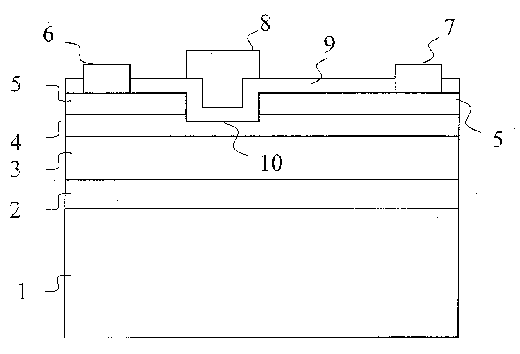
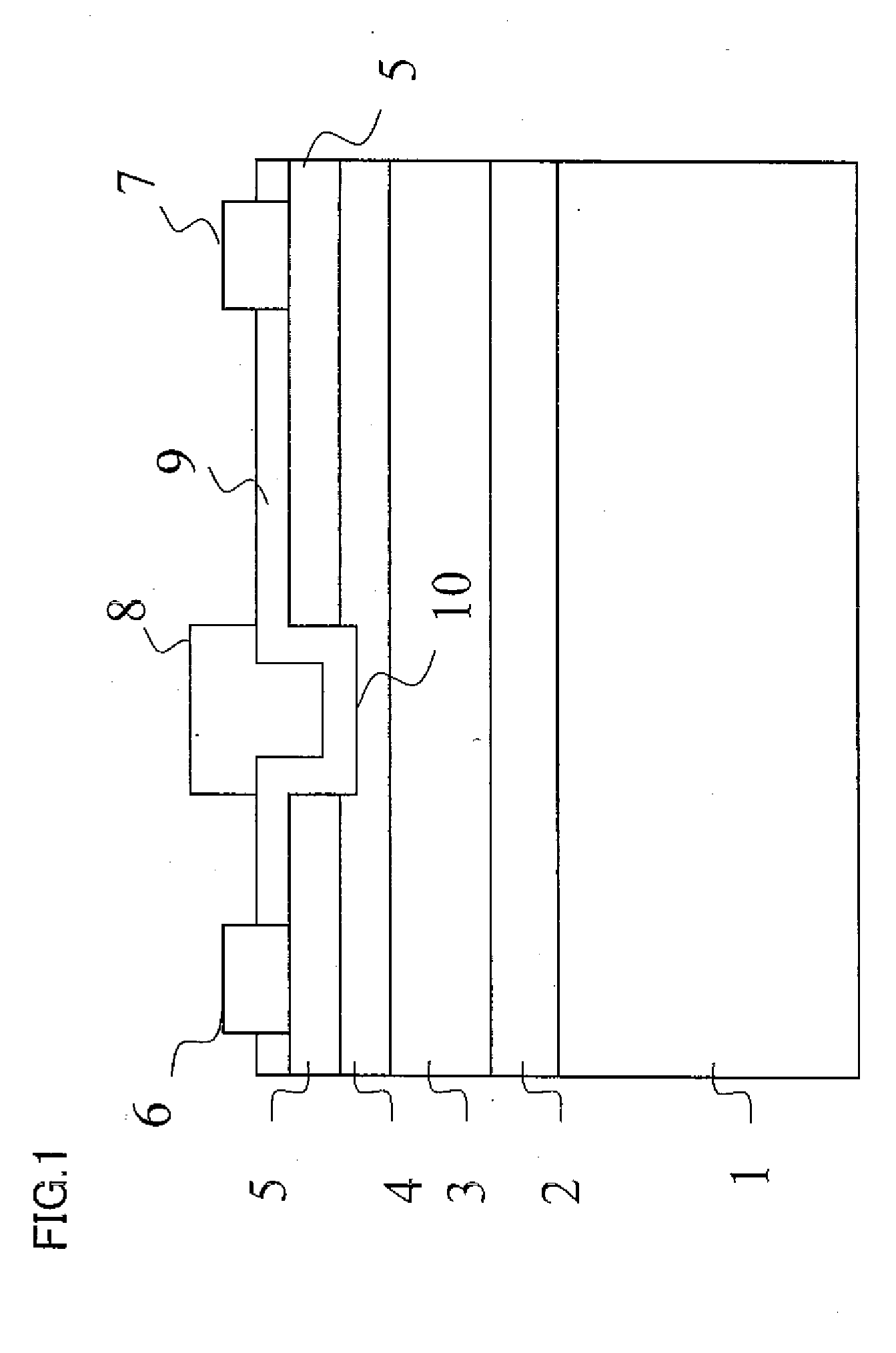
[0031]FIG. 1 shows a schematic cross-sectional view illustrating a nitride semiconductor device of a first embodiment according to the present invention. It should be noted that, in the drawings of the present application, the like reference numerals represent the like components or corresponding components. Further, in the drawings of the present application, dimensional relation between length, width, thickness, and such does not represent actual dimensional relation and is arbitrarily modified for the sake of clarity and simplicity of the drawings.

[0032]The field-effect transistor shown in FIG. 1 includes a substrate 1, a buffer layer 2, a first nitride semiconductor layer 3, a second nitride semiconductor layer 4 as a carrier travel layer, a third nitride semiconductor layer 5 as a barrier layer having a wide band gap compared to second nitride semiconductor layer 4, a source electrode 6, a drain electrode 7, a gate electrode 8, a dielectric film 9, and a recess structure 10.

[00...

second embodiment

[0050]FIG. 6 is a schematic cross-sectional view illustrating a nitride semiconductor device of a second embodiment according to the present invention. The field-effect transistor of FIG. 6 is different from the transistor of FIG. 5 in that first nitride semiconductor layer 3 of p-type GaN is replaced with a first nitride semiconductor layer 13 of p-type InGaN. That is, first nitride semiconductor layer 13 has a narrower band gap as compared with buffer layer 2.

[0051]More specifically, first nitride semiconductor layer 13 is made of p-type In0.1Ga0.9N doped with Mg at a concentration of 1×1019 cm−3, and has a thickness of 50 nm. Further, second nitride semiconductor layer 4 made of undoped GaN is 200 nm thick. First nitride semiconductor layer 13, second nitride semiconductor layer 4, and third nitride semiconductor layer 5 are lattice-matched with a GaN layer as a top layer included in buffer layer 2. Recess area 10 is dug down to a depth of 150 nm from the heterojunction interface...

third embodiment

[0060]FIG. 8 is a schematic cross-sectional view illustrating a nitride semiconductor device of a third embodiment according to the present invention. The field-effect transistor of FIG. 8 is different from the transistor of FIG. 5 in that first nitride semiconductor layer 3 of p-type GaN is replaced with a first nitride semiconductor layer 23 of AlGaN. That is, first nitride semiconductor layer 23 has a wider band gap as compared with the top layer of buffer layer 2 and second nitride semiconductor layer 4.

[0061]More specifically, first nitride semiconductor layer 23 is made of undoped Al0.05Ga0.95N, and has a thickness of 500 nm. Further, second nitride semiconductor layer 4 of undoped GaN is set to be 40 nm thick. Recess area 10 is dug down to a depth of 30 nm from the heterojunction interface between third nitride semiconductor layer 5 and second nitride semiconductor layer 4.

[0062]First nitride semiconductor layer 23 is not limited to AlGaN, and as long as a material having a l...


PUM


Abstract

A nitride semiconductor device includes a first, a second, and a third nitride semiconductor layers that are laminated on a foundation semiconductor layer in stated order, the third nitride semiconductor layer having a wider band gap as compared with the second nitride semiconductor layer, a recess area that is dug from an upper surface of the third nitride semiconductor layer down to a middle of the second nitride semiconductor layer, a first electrode and a second electrode respectively formed on one side and the other side of the recess area so as to be in contact with one of the third nitride semiconductor layer and the second nitride semiconductor layer, a dielectric film formed on the third nitride semiconductor layer and an inner surface of the recess area, and a control electrode formed on the dielectric film in the recess area.

Description

[0001]This nonprovisional application is based on Japanese Patent Application No. 2008-037298 filed on Feb. 19, 2008, with the Japan Patent Office, the entire contents of which are hereby incorporated by reference.BACKGROUND OF THE INVENTION[0002]1. Field of the Invention[0003]The present invention relates to a nitride semiconductor device and a power conversion apparatus including the same, and more particularly to improvement in a nitride semiconductor device suitable for high-power application requiring operation at high voltage and a power conversion apparatus including the same.[0004]2. Description of the Background Art[0005]Semiconductor elements formed with nitride semiconductor material are expected to be useful as power devices capable of acting at high voltage and high current, because of characteristics inherent to the material. Among these elements, field-effect transistors and diodes that utilize an AlGaN / GaN heterojunction attract attention as devices capable of reduci...

Claims


Application Information

Patent Timeline
Patent Type & Authority Applications(United States)
IPC IPC(8): H01L29/205
CPCH01L23/291H01L29/063H01L29/0847H01L29/1083H01L29/1087H01L29/2003H01L29/205H01L2924/0002H01L29/4236H01L29/42376H01L29/7787H01L2924/00
Inventor OKA, TOHRU
Owner SHARP KK
Why Eureka
Try Eureka