A kind of manufacturing method of semiconductor discharge tube

A manufacturing method and technology for discharge tubes, which are applied in semiconductor/solid-state device manufacturing, semiconductor devices, circuits, etc., can solve problems such as increasing production costs, affecting the quality of discharge tubes, stacking faults, etc., and achieving the effect of reducing processes

Active Publication Date: 2017-06-06
SHENZHEN BENCENT ELECTRONICS CO LTD
View PDF4 Cites 0 Cited by
  • Summary
  • Abstract
  • Description
  • Claims
  • Application Information

AI Technical Summary

Problems solved by technology

[0005] However, in the prior art process, deep boron diffusion is generally carried out at 1050-1150°C, at this high temperature, silicon wafers are prone to defects, such as dislocations, stacking faults and other defects, which will lead to leakage current Exceeding the standard seriously affects the quality of the discharge tube
In addition, the deep boron oxidation takes a long time, usually 30-120 hours, which also increases the production cost

Method used


Image

  • A kind of manufacturing method of semiconductor discharge tube

Examples


Embodiment 1

[0030] (1) Perform primary oxidation on both sides of the silicon wafer at the same time to form a primary oxide layer.

[0031] (2) Perform photolithography on the deep boron region of the primary oxide layer of the silicon wafer.

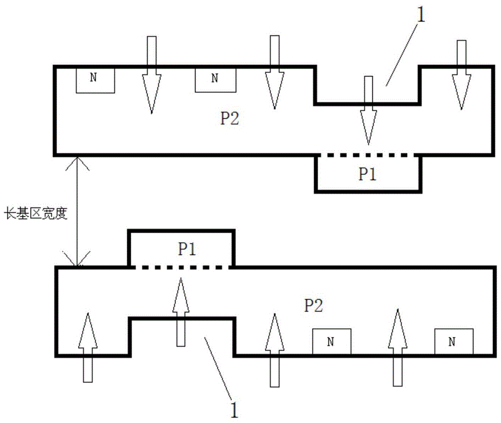
[0032] (3) Etch the surface position of the silicon wafer where the deep boron region is to be formed by using a silicon etching solution, and form a 60 μm deep groove 1 by etching, and the groove 1 corresponds to the shape of the deep boron region, such as figure 1 shown.

[0033] (4) Perform photolithography on the base region of the silicon wafer.

[0034] (5) Carry out light boron diffusion at 1000° C., and the diffusion time is 100 minutes. At the same diffusion rate, the diffusion direction is as figure 1 As shown by the middle arrow, due to the existence of groove 1 formed by corrosion, the junction depth of boron diffusion in groove 1 will be greater than that of boron diffusion in other parts, forming a protrusion (the protrusion dista...

Embodiment 2

[0044] (1) Perform primary oxidation on both sides of the silicon wafer at the same time to form a primary oxide layer.

[0045] (2) Perform photolithography on the deep boron region of the primary oxide layer of the silicon wafer.

[0046] (3) Etch the surface position of the silicon wafer where the deep boron region is to be formed by using a silicon etching solution, and form a 55 μm deep groove by etching, and the groove corresponds to the shape of the deep boron region, such as figure 1 shown.

[0047] (4) Perform photolithography on the base region of the silicon wafer.

[0048] (5) Carry out light boron diffusion at 950° C., and the diffusion time is 60 minutes. At the same diffusion rate, the diffusion direction is as figure 1 As shown by the middle arrow, due to the existence of the groove formed by corrosion, the junction depth of boron diffusion in the groove will be larger than that of the boron diffusion area in other parts, forming a protruding (protruding dis...

Embodiment 3

[0058] (1) Perform primary oxidation on both sides of the silicon wafer at the same time to form a primary oxide layer.

[0059] (2) Perform photolithography on the deep boron region of the primary oxide layer of the silicon wafer.

[0060] (3) Etch the surface position of the silicon wafer where the deep boron region is to be formed by using a silicon etching solution, and form a 45 μm deep groove by etching, and the groove corresponds to the shape of the deep boron region, such as figure 1 shown.

[0061] (4) Perform photolithography on the base region of the silicon wafer.

[0062] (5) Carry out light boron diffusion at 1050° C., and the diffusion time is 90 minutes. At the same diffusion rate, the diffusion direction is as figure 1 As shown by the middle arrow, due to the existence of the groove formed by corrosion, the junction depth of boron diffusion in the groove will be greater than that of the boron diffusion area in other parts, forming a protruding (protruding d...


PUM

PropertyMeasurementUnit
depthaaaaaaaaaa

Abstract

The invention discloses a manufacturing method of a semiconductor discharge tube. The manufacturing method comprises the following steps: (1), performing primary oxidation on a silicon wafer; (2), photoetching a deep-boron area of the silicon wafer; (3), etching the position which is to be formed into the deep-boron area by use of a silicon etch solution so as to form a groove, wherein the groove corresponds to the shape of the deep-boron area; (4) photoetching a base area; (5), performing diluted boron diffusion; (6), performing diluted boron oxidation; (7),photoetching an emitting area; (8), performing phosphor diffusion; (9), performing phosphor oxidation; (10), performing double-sided lead photoetching; (11), performing double-sided metallization on the silicon wafer; (12), photoething metal; and (13), alloying the silicon wafer under a vacuum state. According to the manufacturing method, deep-boron effect is realized by virtue of a corrosion structure combining diluted boron diffusion, and processes are reduced, the cost is greatly saved, detects such as dislocation and stacking fault of the silicon wafer due to a high temperature in the deep boron process are also avoided, and thus the problem that current leakage exceeds the standard can not be caused.

Description

technical field [0001] The invention relates to a method for manufacturing a semiconductor discharge tube, which belongs to the technical field of semiconductor discharge tube manufacturing technology. Background technique [0002] The semiconductor discharge tube is an overvoltage protection device. It relies on the breakdown current of the PN junction to trigger the device to conduct and discharge, and can flow a large surge current or pulse current. When in use, the semiconductor discharge tube can be directly connected across the protected The two ends of the circuit, in the range of its breakdown voltage, constitute the range of overvoltage protection. [0003] In order to obtain a better lightning strike and power frequency effect under the condition that the thickness of the semiconductor discharge tube remains unchanged, the general technical method is to carry out boron deepening on a part of the silicon wafer. The local boron deepening reduces the width of the lon...

Claims


Application Information

Patent Timeline
Patent Type & Authority Patents(China)
IPC IPC(8): H01L21/22
CPCH01L21/22H01L21/30604H01L29/66363
Inventor 陈林刘志雄
Owner SHENZHEN BENCENT ELECTRONICS CO LTD
Why Eureka
Try Eureka