Semiconductor device and a method of manufacturing the same

a technology of semiconductor devices and semiconductors, applied in semiconductor devices, semiconductor/solid-state device details, electrical apparatus, etc., can solve the problems of degrading the precision of detecting marks, and achieve the effect of improving the visibility of alignment marks

Active Publication Date: 2009-08-20
RENESAS ELECTRONICS CORP
View PDF5 Cites 77 Cited by
  • Summary
  • Abstract
  • Description
  • Claims
  • Application Information

AI Technical Summary

Benefits of technology

[0012]The effect brought about by a typical embodiment of the inventions disclosed in the present application will be briefly described as follows.
[0013]Accordin

Problems solved by technology

Consequently, the difference in contrast between the mark and the background region is not even between different semiconductor wafers or between chip regions of the same sem

Method used


Image

  • Semiconductor device and a method of manufacturing the same
  • Semiconductor device and a method of manufacturing the same
  • Semiconductor device and a method of manufacturing the same

Examples


first embodiment

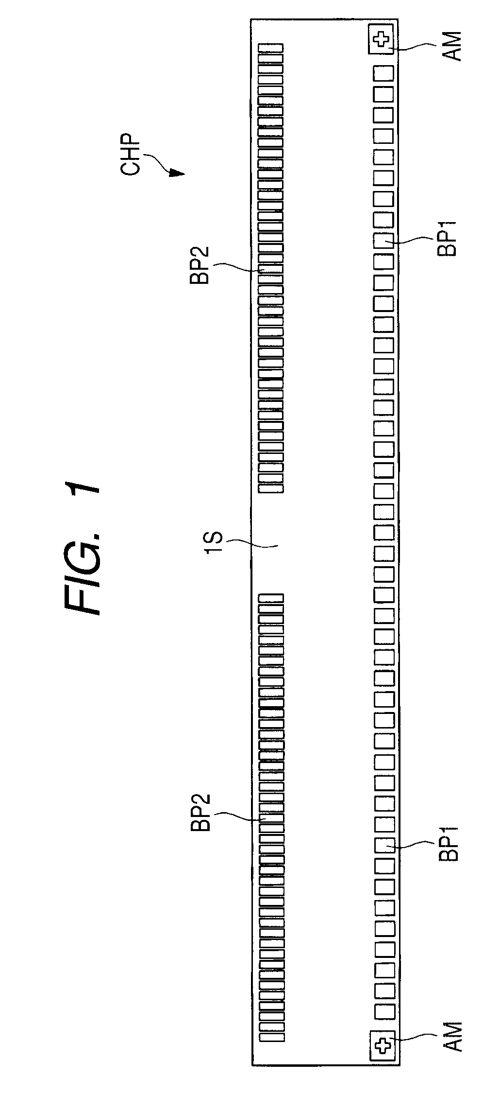
[0052]FIG. 1 is a plan view showing a configuration of a semiconductor chip CHP (semiconductor device) in a first embodiment. The semiconductor chip CHP in the first embodiment is an LCD driver. In FIG. 1, the semiconductor chip CHP has a semiconductor substrate 1S formed into, for example, an elongated oblong shape (rectangular shape) and over its main surface, an LCD driver to drive, for example, a liquid crystal display device is formed. The LCD driver has a function to control the orientation of the liquid crystal molecule by supplying a voltage to each pixel of the cell array constituting the LCD and comprises a gate drive circuit, a source drive circuit, a liquid crystal drive circuit, a graphic RAM (Random Access Memory), a peripheral circuit, etc. These functions are realized by semiconductor devices and wirings formed on the semiconductor substrate 1S. First, a surface configuration of the semiconductor chip CHP will be described.

[0053]The semiconductor chip CHP has a recta...

second embodiment

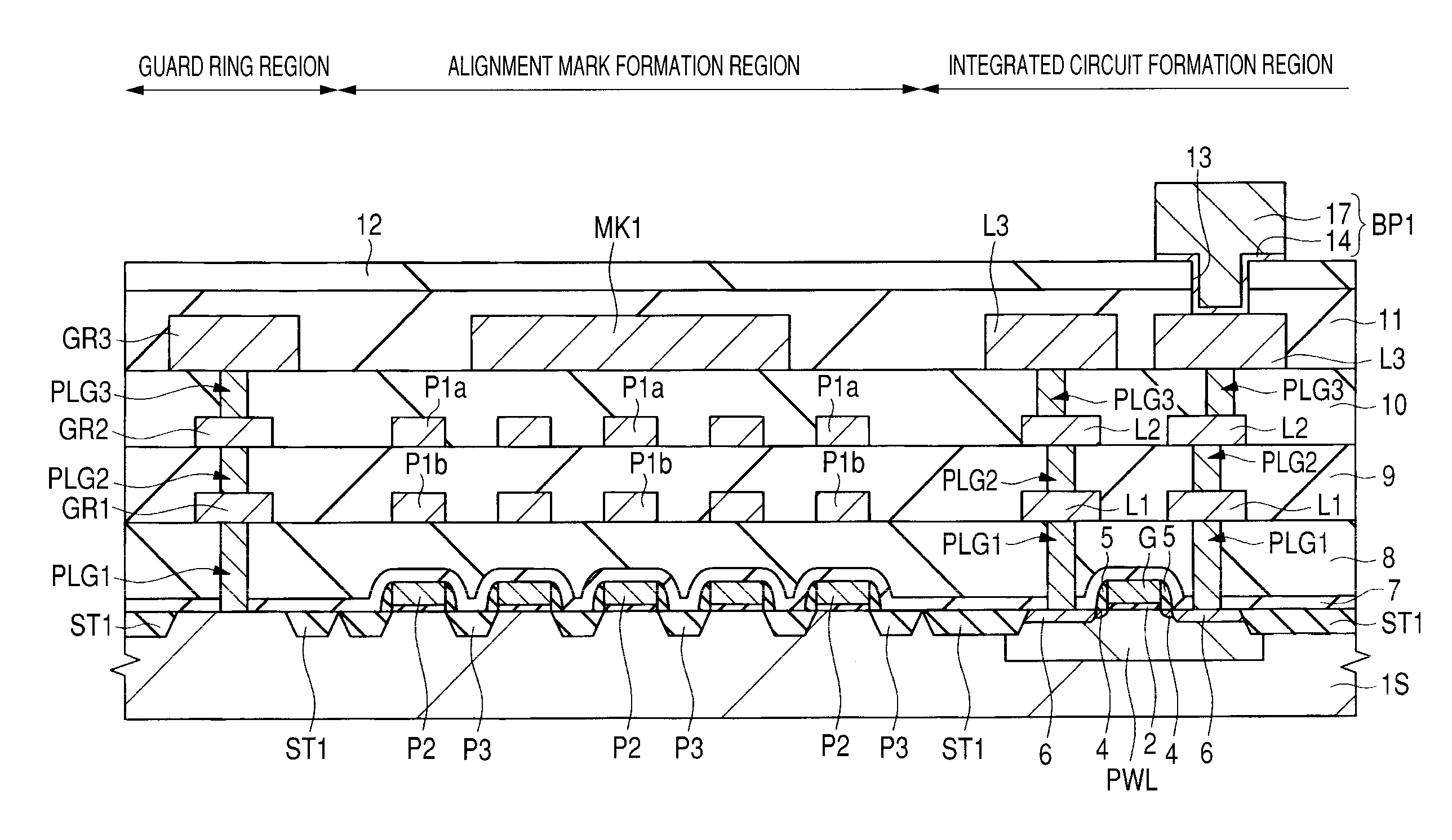
[0143]In the first embodiment described above, as shown in FIG. 7 and FIG. 8, the pattern P1a and the pattern P3 formed in the different layers are arranged so that they overlap in a planar manner (refer to FIG. 7) and the pattern P1b and the pattern P2 formed in the different layers are arranged so that they overlap in a planar manner (refer to FIG. 8). In contrast to this, in a second embodiment, an example will be described, in which the patterns P1a, P1b and P2 formed in the different layers are arranged so that they overlap in a planar manner but not overlap the pattern P3 in a planar manner.

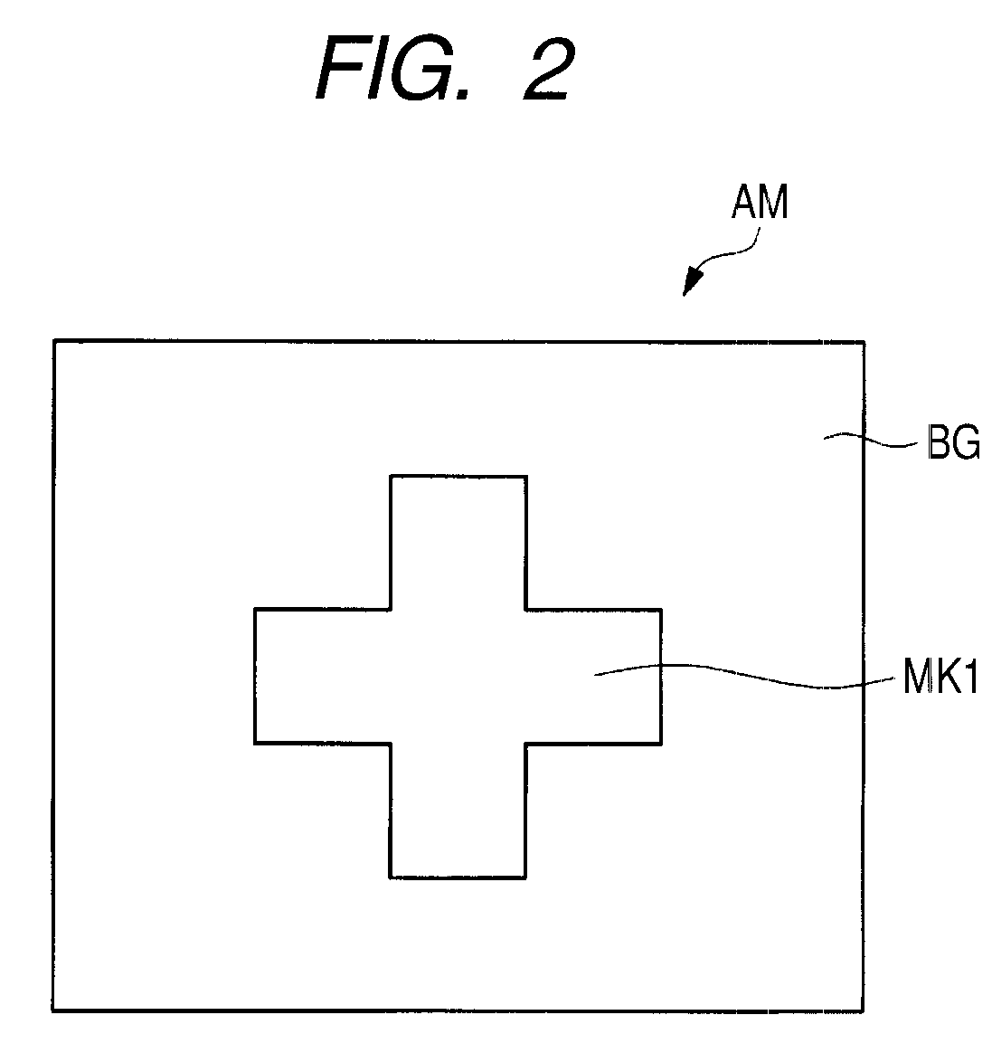
[0144]FIG. 30 is a plan view showing a configuration of the alignment mark AM in the second embodiment. In the alignment mark AM in the second embodiment, the cross-shaped mark MK1 is formed in the center of the rectangular background region BG. Then, in the lower layer of the background region BG including the lower layer of the mark MK1, the dot pattern is formed. The dot pattern shown in...


PUM


Abstract

To provide a technique capable of positioning of a semiconductor chip and a mounting substrate with high precision by improving visibility of an alignment mark. In a semiconductor chip constituting an LCD driver, a mark is formed in an alignment mark formation region over a semiconductor substrate. The mark is formed in the same layer as that of an uppermost layer wiring (third layer wiring) in an integrated circuit formation region. Then, in the lower layer of the mark and a background region surrounding the mark, patterns are formed. At this time, the pattern P1a is formed in the same layer as that of a second layer wiring and the pattern P1b is formed in the same layer as that of a first layer wiring. Further, the pattern P2 is formed in the same layer as that of a gate electrode, and the pattern P3 is formed in the same layer as that of an element isolation region.

Description

CROSS-REFERENCE TO RELATED APPLICATION[0001]The present application claims priority from Japanese patent application No. 2008-32666 filed on Feb. 14, 2008, the content of which is hereby incorporated by reference into this application.BACKGROUND OF THE INVENTION[0002]The present invention relates to a semiconductor device and a method of manufacturing the same and more particularly to a technique which is useful for the application to an LCD (Liquid Crystal Display) driver that drives a liquid crystal display unit and manufacturing thereof.[0003]In Japanese patent laid-open No. 11-330247 (patent document 1), a technique is described, which can accurately detect an alignment mark when forming an alignment mark for laser trimming within a chip. Specifically, the surface of a semiconductor substrate made of SOI substrate has a tapered part oblique with respect to the normal direction at least in the peripheral region of the alignment mark and laser light is caused to reflect in a direc...

Claims


Application Information

Patent Timeline
IPC IPC(8): H01L29/78H01L23/544H01L21/8234
CPCH01L23/544H01L23/585H01L2924/1306H01L23/535H01L29/78H01L24/29H01L24/83H01L2223/5442H01L2223/54426H01L2223/5448H01L2224/16H01L2224/83101H01L2224/838H01L2924/01005H01L2924/01013H01L2924/01015H01L2924/01027H01L2924/01029H01L2924/01033H01L2924/0104H01L2924/01046H01L2924/01047H01L2924/01054H01L2924/01057H01L2924/01073H01L2924/01074H01L2924/01078H01L2924/01079H01L2924/01082H01L2924/04941H01L2924/0781H01L2924/14H01L2924/19043H01L2924/30105H01L2924/3025H01L2924/0132H01L2924/01006H01L2924/01019H01L2924/01041H01L2924/01072H01L2924/01022H01L2924/00H01L2924/12042H01L2924/15788H01L21/00H01L23/5226H01L23/5283H01L24/13H01L24/81H01L27/124H01L27/1248H01L2224/8113H01L2224/8185H01L2924/1426H01L2924/1433
Inventor KOKETSU, MASAMISAWADA, TOSHIAKI
Owner RENESAS ELECTRONICS CORP
Why Eureka
Try Eureka