Solid-state imaging device, camera, and electronic device

a technology of solid-state imaging and electronic devices, which is applied in the direction of radio frequency controlled devices, television system scanning details, television systems, etc., can solve the problems of image quality degradation and image quality degradation, and achieve the reduction of resistance and capacitance, focusing efficiency, and wiring density on other layers.

Inactive Publication Date: 2009-08-20
SONY CORP
View PDF3 Cites 11 Cited by
  • Summary
  • Abstract
  • Description
  • Claims
  • Application Information

AI Technical Summary

Benefits of technology

[0022]In a CMOS image sensor, several wirings in the pixel array are provided using metal wirings for driving pixel transistors, pixel output, power supply, and grounding circuits. In the so-called front-illuminated CMOS image sensor in which light is incident on the photoelectric conversion element from the side provided with wirings formed thereon, it may be necessary to prevent the decrease in sensitivity caused by vignetting due to wirings. In addition, in order to improve the sensitivity by increasing the focusing efficiency, it is desirable to reduce a device height by reducing the distance between the photoelectric conversion element and on-chip lens.

Problems solved by technology

These may result in the degradation of image quality.
The characteristics of the pixel vary with the location in the imaging region, and the degradation of image quality due to the shading and the like may take place.

Method used


Image

  • Solid-state imaging device, camera, and electronic device
  • Solid-state imaging device, camera, and electronic device
  • Solid-state imaging device, camera, and electronic device

Examples


Embodiment Construction

[0049]Embodiments of the present invention will be described hereinbelow by referring to the accompanying drawings.

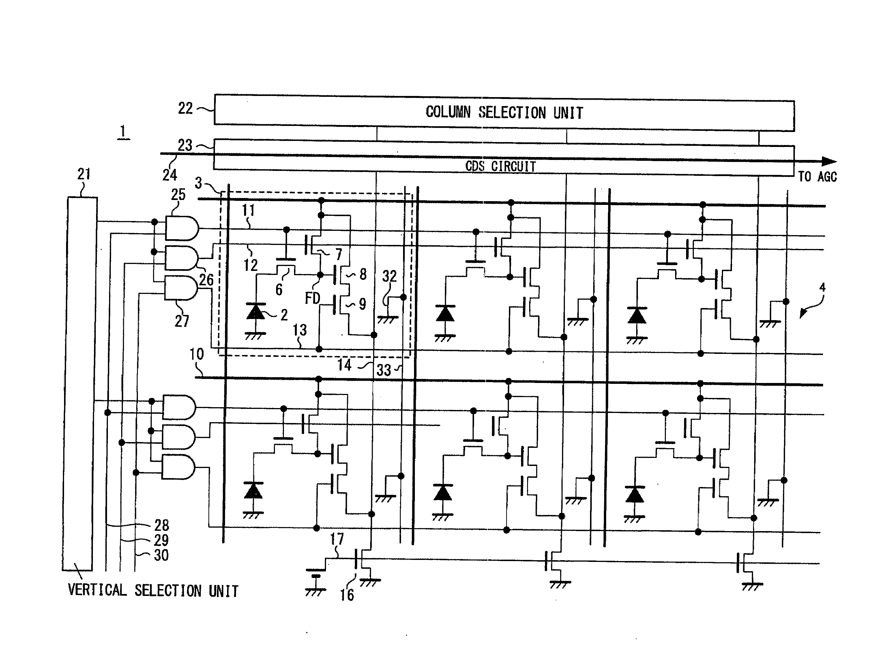
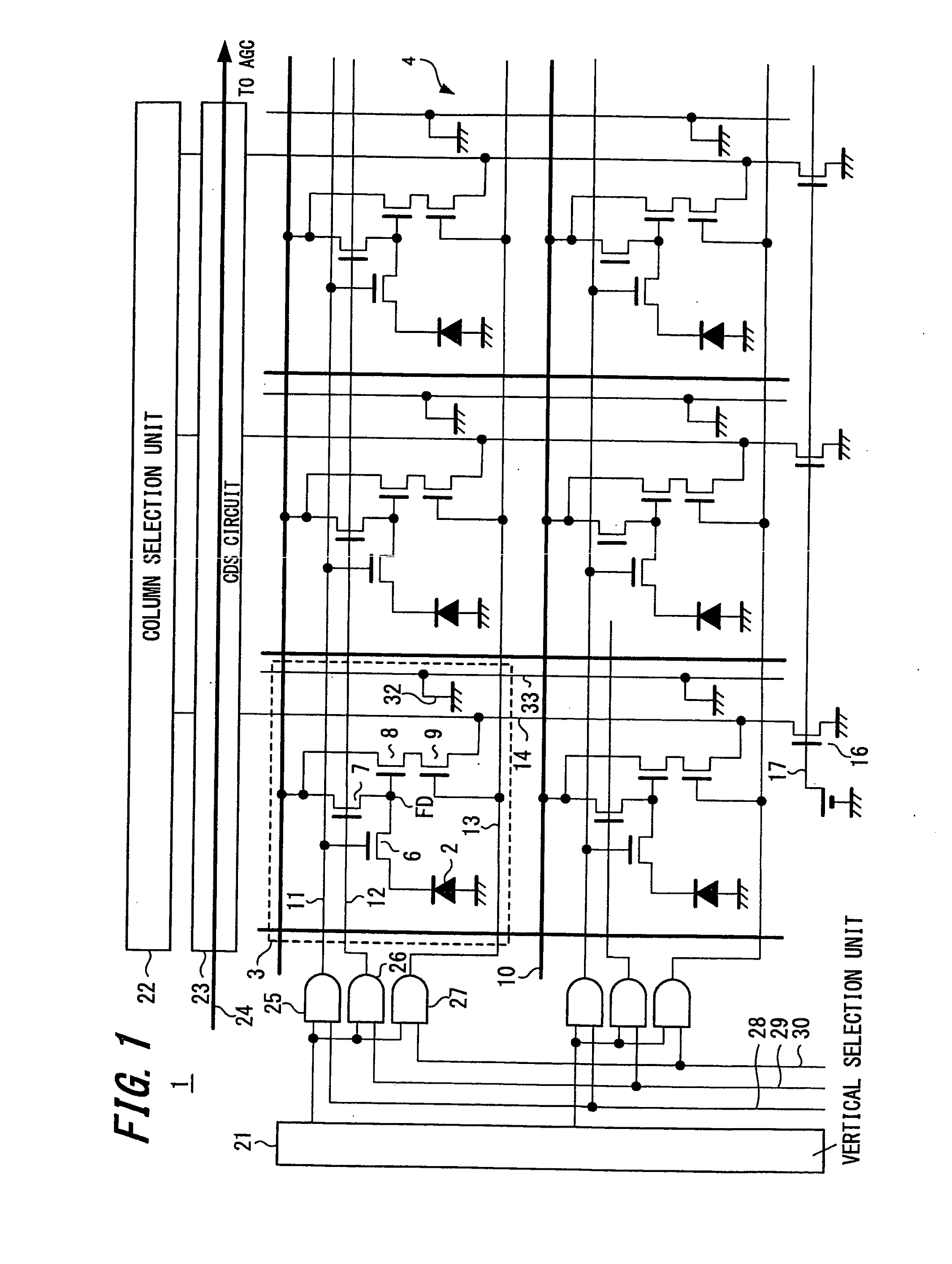
[0050]A solid-state imaging device according to an embodiment of the present invention may be a typical front-illuminated CMOS image sensor. Although examples of the solid-state imaging device according to an embodiment of the invention are described hereinbelow with the illustration assuming the aforementioned configuration diagrammatically shown in FIG. 1, it is not intended to limit the invention to the illustration and accompanied drawings.

[0051]The schematic configuration of the solid-state imaging device as a CMOS image sensor according to an embodiment of the invention is similar to that illustrated in FIG. 1. That is, the solid-state imaging device according to the present embodiment includes an imaging section and peripheral circuits disposed around the imaging section. The imaging section includes a plurality of pixels (unit cells) arranged in a two-dimensiona...


PUM


Abstract

Disclosed is a solid-state imaging device which includes an imaging region including pixels arranged two-dimensionally, each of the pixels including a photoelectric conversion element and a plurality of pixel transistors for reading out signals outputted from the photoelectric conversion element, and wirings formed on stacked layers for driving each of the pixels. A shading part between the pixels is formed by combining first and second wirings selected from the wirings.

Description

CROSS REFERENCES TO RELATED APPLICATIONS[0001]The present invention contains subject matter related to Japanese Patent Application JP 2008-035361 filed in the Japanese Patent Office on Feb. 15, 2008, the entire contents of which being incorporated herein by reference.BACKGROUND OF THE INVENTION[0002]1. Field of the Invention[0003]The invention generally relates to solid-state imaging devices, cameras, and electronic devices. More particularly the invention relates to a solid-state imaging device including in a pixel a convertor for converting electric charges generated by a photoelectric conversion element to pixel signals, such as CMOS image sensor, for example. The invention also relates to a camera and an electronic device each provided with the solid-state imaging device. The CMOS image sensor is referred herein to an image sensor fabricated at least partially utilizing the CMOS process.[0004]2. Description of the Related Art[0005]A CMOS image sensor is a solid-state imaging dev...

Claims


Application Information

Patent Timeline
Patent Type & Authority Applications(United States)
IPC IPC(8): H04N5/335H01L27/146H04N5/351H04N5/361H04N5/369H04N5/374
CPCH04N5/3572H01L27/14603H04N25/61H04N25/76
Inventor ABE, TAKASHISUZUKI, RYOJI
Owner SONY CORP
Why Eureka
Try Eureka