Method and apparatus for inspecting defect of pattern formed on semiconductor device

a technology of pattern formation and semiconductor, applied in the direction of semiconductor/solid-state device testing/measurement, image enhancement, instruments, etc., can solve the problems of pattern shape itself (systematic defect) which cannot be detected by comparison of image to image of such actual pattern, and achieve the effect of improving the accuracy of defect inspection

Active Publication Date: 2009-08-20
HITACHI HIGH-TECH CORP
View PDF1 Cites 38 Cited by
  • Summary
  • Abstract
  • Description
  • Claims
  • Application Information

AI Technical Summary

Benefits of technology

[0015]A normal circuit pattern has an allowable range of a certain degree, therefore it is difficult to judge a defect by comparison with one comparison shape. Also, the factor of shape deformation is not one but combination of a plurality of defect occurrence factors in general, therefore, it is difficult to presume the shape variation based on one rule. In order to address such problem, variation of the normal shape is formed taking the supposed defect occurrence factor into consideration, thereby it becomes possible to detect even the defect caused by combination of a plurality of factors with high accuracy.
[0025]In accordance with the present invention, the user can adjust the density of the shape variation in formation of the comparison shape set, and reflection of the user's needs in trade-off of the inspection time and inspection accuracy becomes possible.
[0027]In accordance with the present invention, deformation of the circuit shape by variation of the exposure condition can be reproduced more faithfully, which leads to improvement of accuracy in defect inspection.
[0028]According to the present invention, the following effects can be realized.(1) Even for the defect where a plurality of factors are combined, detection of the defect or classification according to respective occurrence factor becomes possible, and failure remedy can be made speedy.(2) Even if a defect caused by a non-supposed factor is mixed in, more detailed classification can be performed by analysis of the shape deviation at the defect portion extracted accurately.(3) Automatic classification of large numbers of SEM images according to respective defect occurrence factor becomes possible with the circuit pattern images and circuit design data, which leads to speedy failure remedy.

Problems solved by technology

In recent years, as semiconductor circuit becomes complicated and refined in dimension, drop of yield due to frequent occurrence of patterning failure originating the manufacturing process of the semiconductor has become a problem.
However, as refinement and densification of the circuit pattern progress, the defect of the pattern shape itself (systematic defect) which cannot be detected by comparison of image to image of such actual pattern has started to occur.
Therefore, even if one standard pattern is formed for comparison imitating a normal shape, as in the pattern inspection method described in Japanese Unexamined Patent Application Publication No. 2005-277395, the shape may not necessarily be suitable for detection of the defect.
In addition, with respect to the defect occurring by combination of a plurality of process variation factors, it is difficult to find out its occurrence factor.

Method used


Image

  • Method and apparatus for inspecting defect of pattern formed on semiconductor device
  • Method and apparatus for inspecting defect of pattern formed on semiconductor device
  • Method and apparatus for inspecting defect of pattern formed on semiconductor device

Examples


embodiment 1

[0054]As Embodiment 1, an embodiment will be described wherein variation of exposure condition is made a supposed defect occurrence factor and detection and classification according to the respective occurrence factor of the defect are performed.

[Total Parts Constitution]

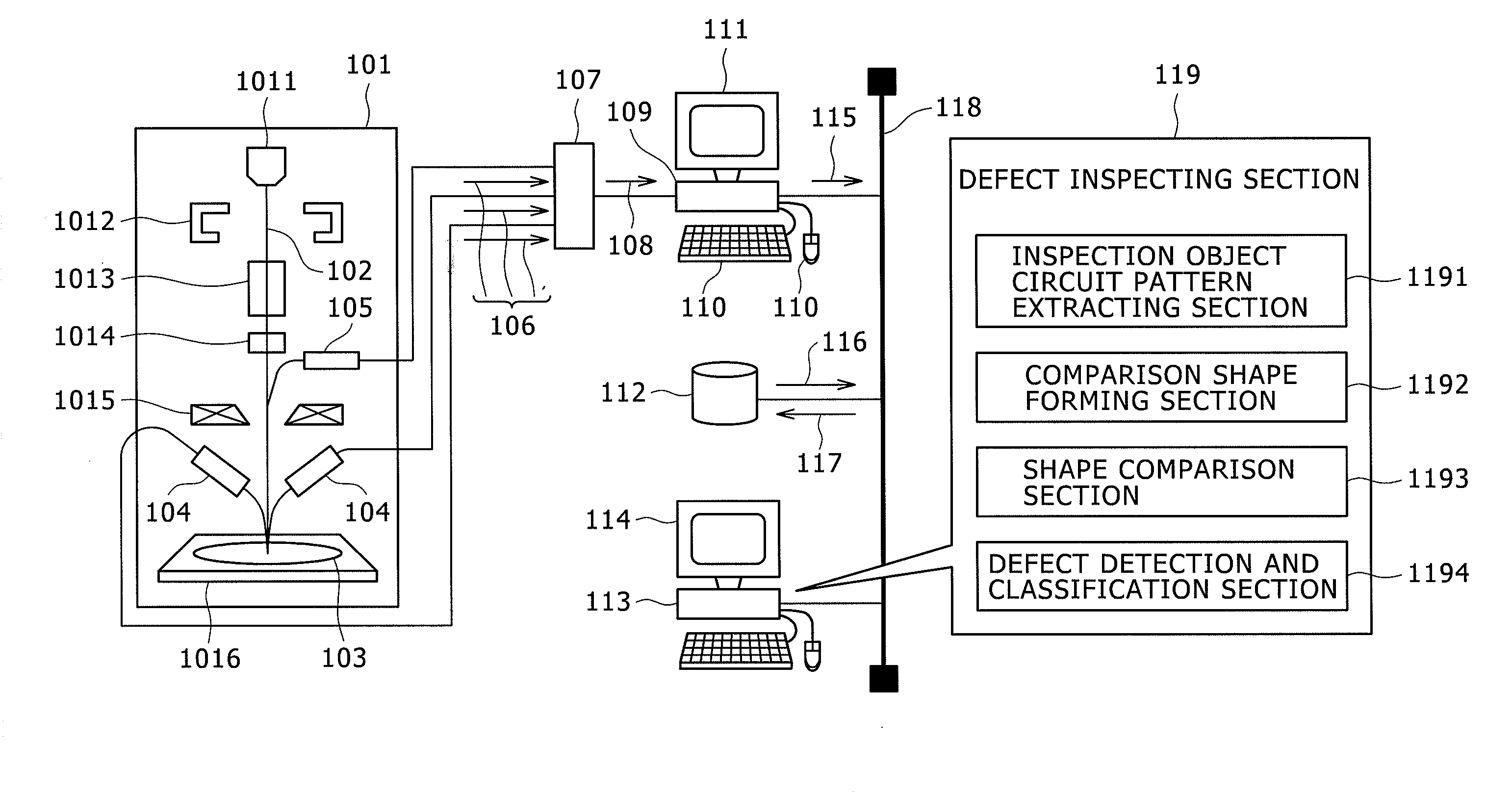
[0055]FIG. 1 is a schematic constitution drawing of the defect inspection apparatus with a SEM for detection and classification of the defect on a semiconductor wafer in accordance with an embodiment of the present invention.

[0056]101 is a SEM comprising in its inside; an electron source 1011, an extraction electrode 1012 for extracting an electron emitted from the electron source 1011 by desired acceleration energy in a beam shape, scanning electrodes 1013, 1014 for scanning an electron beam 102 extracted by the extraction electrode 1012 by the desired acceleration energy in a beam shape two-dimensionally in X or Y direction, a lens electrode 1015 for adjusting the focusing position of the electron beam 102 in orde...

embodiment 2

[0106]As Embodiment 2, an embodiment will be described wherein variation of exposure condition and an error in an overlay position occurring between layers are made supposed defect occurrence factors, and detection and classification are performed with respect to an abnormal exposure condition defect, an overlay position error defect, and a defect caused by a plurality of non-supposed defect occurrence factors. As the present embodiment is similar to Embodiment 1 with respect to apparatus constitution and process steps, only the points different in processing contents will be described.

[0107]FIG. 20 is an explanatory drawing of a comparison shape forming section in accordance with the present embodiment. Here, explanation will be made using double layer design data. Based on design data 2001, a comparison shape set 2004 is formed by the comparison shape forming section 1192. At this time, shape deformation is performed in accordance with an exposure condition variation shape deforma...

embodiment 3

[0111]As Embodiment 3, an embodiment will be described referring to FIG. 17 wherein defect detection and classification is performed when the number of supposed defect occurrence factors is made optional.

[0112]First, in a comparison shape forming section 1702, a comparison shape set 1703 is formed based on design data 1701. The comparison shape set 1703 is a group of a plurality of shapes added with deformation according to predetermined shape deformation rules 1711. The shape deformation rules 1711 are to stipulate a deformation method 17111 of the design data (information on deformation variation such as a deformation range 17112, and deformation quantity step 17113, for example) according to respective supposed defect occurrence factor such as variation of exposure condition, an error of an overlay position occurring between layers, and an overlay error in a multi-layer pattern, and can stipulate any number of variations. A deformation quantity set 1712 is an optional combination...


PUM


Abstract

In the inspection apparatus for a defect of a semiconductor and the method using it for automatically detecting the defect on a semiconductor wafer and presuming the defect occurrence factor using the circuit design data, a plurality of shapes are formed from the circuit design data by deforming the design data with respect to shape deformation items stipulated for respective defect occurrence factor for comparison with the inspection object circuit pattern. The defect is detected by comparison of the group of shapes formed and the actual pattern. Further, the occurrence factors of these defects are presumed, and the defects are classified according to respective factor.

Description

BACKGROUND OF THE INVENTION[0001]1. Field of the Invention[0002]The present invention relates to an apparatus for observing in detail and classifying a defect on a semiconductor wafer detected by another inspection apparatus, in particular, relates to an apparatus and a method for inspecting a semiconductor defect for detecting patterning failure based on an image of a circuit pattern formed on the semiconductor wafer and further classifying the defect based on the defect occurrence factor.[0003]2. Description of the Related Art[0004]In recent years, as semiconductor circuit becomes complicated and refined in dimension, drop of yield due to frequent occurrence of patterning failure originating the manufacturing process of the semiconductor has become a problem. Also, because the factors of failures hidden in the manufacturing process are diversified, it is desired to automate the work for detecting the defect on the semiconductor wafer and determining the factor of the defect in ord...

Claims


Application Information

Patent Timeline
Patent Type & Authority Applications(United States)
IPC IPC(8): G06K9/00G06V10/772
CPCG06K9/6255G06T7/001G06T2207/10056G06T2207/30148H01L2924/0002H01L22/12H01L2924/00G06V10/772G06F18/28
Inventor NISHIURA, TOMOFUMIMIYAMOTO, ATSUSHISHISHIDO, CHIESUTANI, TAKUMICHI
Owner HITACHI HIGH-TECH CORP
Why Eureka
Try Eureka