Thin film transistor and method for forming the same

a thin film transistor and transistor technology, applied in the field of thin film transistors, can solve the problems of reducing the output light of the diode, the active layer 34 is not electrically stable, and the driving current through the diode is not stable, so as to reduce the off-current and the effect of reducing the off-curren

Inactive Publication Date: 2009-08-27
IGNIS INNOVATION
View PDF3 Cites 32 Cited by
  • Summary
  • Abstract
  • Description
  • Claims
  • Application Information

AI Technical Summary

Benefits of technology

[0012]It is an object of the invention to provide a TFT and a method of forming the TFT that obviates or mitigates at least one of the disadvantages of existing systems.
[0013]According to an aspect of the present invention there is provided a method of forming a thin film transistor on a surface of a substrate, includes the steps of: forming a gate electrode; deposing a gate dielectric on the gate electrode; forming a nanocrystalline silicon (nc-Si) layer and an amorphous silicon (a-Si:H) layer above the gate dielectric, so that the thickness of the nc-Si layer is less than 30 nm thereby reducing off-current; and forming a source / drain electrode.
[0014]According to another aspect of the present invention there is provided a TFT includes: a gate electrode on a substrate, a gate dielectric on the gate electrode; a nc-Si layer having a thickness less than 30 nm, thereby reducing off-current; an a-Si:H layer; and a source / drain electrode.

Problems solved by technology

However, in this conventional TFT, the a-Si:H active layer 34 is not electrically stable, i.e. the threshold voltage of the TFT changes under applied gate voltage.
This leads to a decrease in the driving current through the diode and, consequently, a decrease in the output light by the diode.
The oxygen-containing plasma uses gases such as N2O, NO, NO2, H2O2 which are not compatible with the standard mainstream TFT technology and leads to process complexity and cost.
A further drawback is that all these gases are considered greenhouse gases.

Method used


Image

  • Thin film transistor and method for forming the same
  • Thin film transistor and method for forming the same
  • Thin film transistor and method for forming the same

Examples


Embodiment Construction

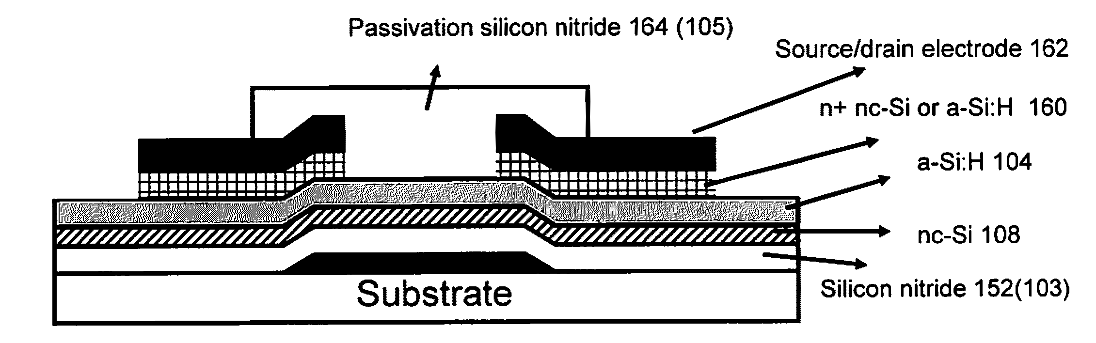
[0028]Embodiments of the present invention describe a TFT that includes a patterned gate electrode on a substrate, a gate dielectric formed on the gate electrode, a nc-Si layer, an a-Si:H layer (cap layer), and a passivation dielectric or silicon nitride layer.

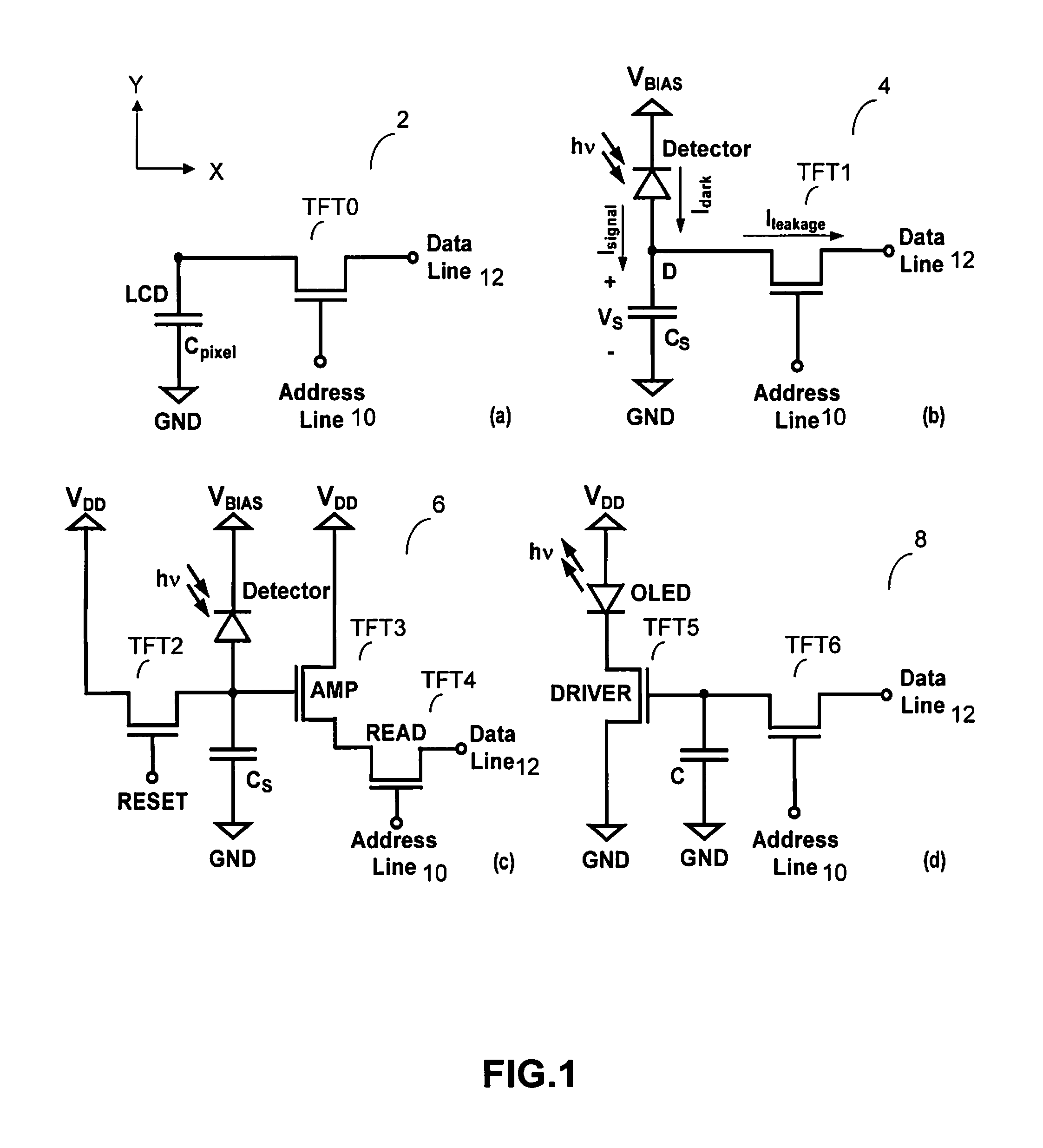
[0029]The TFT in accordance with the embodiments of the present invention may be used for displays and imagers, including those of FIGS. 1(a)-(d). The TFT in accordance with the embodiments of the present invention may be used for active matrix flat panel electronics.

[0030]As described in detail below, the method of forming the nc-Si layer on the gate dielectric is fully compatible with the standard fabrication processes while the nanocrystals form at the interface with the gate dielectric which results in reduced threshold voltage shift of the TFT. Furthermore, the a-Si:H and the nc-Si layer with a proper thickness described below minimizes the TFT source-drain leakage current (off-current) without compromising the TFT drive ...


PUM


Abstract

A thin film transistor (TFT) and the method of forming the same is provided. The method of forming the TFT on a surface of a substrate, includes the steps of: forming a gate electrode; deposing a gate dielectric on the gate electrode; forming a nanocrystalline silicon (nc-Si) layer and an amorphous silicon (a-Si:H) layer above the gate dielectric, so that the thickness of the nc-Si layer is less than 30 nm thereby reducing off-current; and forming a source/drain electrode. The TFT includes: a gate electrode on a substrate, a gate dielectric on the gate electrode; a nc-Si layer having a thickness less than 30 nm, thereby reducing off-current; an a-Si:H layer; and a source/drain electrode.

Description

CROSS-REFERENCE TO RELATED APPLICATIONS[0001]The present application claims priority to provisional application Ser. No. 60 / 983,824 filed on Oct. 30, 2007, and is incorporated by reference herein in its entirety.FIELD OF INVENTION[0002]The invention relates to a semiconductor technology, and more specifically to a thin film transistor (TFT) and a method of forming the same for active matrix thing film electronics.BACKGROUND OF THE INVENTION[0003]Current interest in active matrix pixilated arrays extends well beyond the ubiquitous active matrix liquid crystal display (AMLCD), that is routinely used as lap top and desk top screens, to several newly emerging and technologically important application areas. Notable examples include linear and area arrays for document scanning, digital copiers, and fax machines, bio-medical x-ray and optical imagers, radio-frequency interrogation tags, and non-destructive testing of material / structural integrity. More significantly, the TFT active matrix...

Claims


Application Information

Patent Timeline
Patent Type & Authority Applications(United States)
IPC IPC(8): H01L29/786H01L21/336
CPCH01L29/04H01L29/78696H01L29/7866H01L29/66765
Inventor NATHAN, AROKIASAZONOV, ANDREIRAD, MOHAMMED REZA ESMAEILI
Owner IGNIS INNOVATION
Why Eureka
Try Eureka