Thin film transistor

a transistor and thin film technology, applied in the field of field-effect transistors, can solve the problems of high manufacturing cost, inability to obtain sufficient switching characteristics, and low field-effect mobility and small on-current, and achieve the effect of small off-current and high productivity

Active Publication Date: 2010-09-09
SEMICON ENERGY LAB CO LTD
View PDF24 Cites 14 Cited by
  • Summary
  • Abstract
  • Description
  • Claims
  • Application Information

AI Technical Summary

Benefits of technology

[0008]A glass substrate for manufacturing display panels has grown in size from year to year as follows: the 3rd generation (550 mm×650 mm), the 3.5th generation (600 mm×720 mm or 620 mm×750 mm), the 4th generation (680 mm×880 mm or 730 mm×920 mm), the 5th generation (1100 mm×1300 mm), the 6th generation (1500 mm×1850 mm), the 7th generation (1870 mm×2200 mm), and the 8th generation (2200 mm×2400 mm). From now on, the size of the glass substrate is expected to grow to the 9th generation (2400 mm×2800 mm or 2450 mm×3050 mm) and the 10th generation (2950 mm×3400 mm). The increase in size of the glass substrate is based on the concept of minimum cost design.
[0010]Therefore, it is an object of an embodiment of the present invention to provide a method for manufacturing a thin film transistor which has favorable electric characteristics with high productivity.
[0018]In addition, in the mixed layer and the layer containing an amorphous semiconductor, dangling bonds of semiconductor atoms which exist at the interface between adjacent microcrystalline semiconductor regions (i.e., crystal grain boundaries) and the interface between the microcrystalline semiconductor region and the amorphous semiconductor region are cross-linked with an NH group and thus defect levels are reduced, so that a path through which carriers are transferred is formed. Alternatively, a dangling bond is terminated with an NH2 group and thus defect levels are reduced.
[0019]As a result, in the thin film transistor, resistance between the gate insulating layer and the source and drain regions of when voltage is applied to a source or drain electrode can be reduced, whereby on-current and field-effect mobility of the thin film transistor can be increased. The layer containing an amorphous semiconductor is formed using a well-ordered semiconductor layer which has fewer defects and whose tail of a level at a band edge in the valence band is steep; therefore, the band gap gets wider, and tunneling current does not easily flow. Therefore, by providing the layer containing an amorphous semiconductor on the back channel side, off-current of the thin film transistor can be reduced.
[0023]As described above, a thin film transistor with small off-current and large on-current can be manufactured with high productivity.

Problems solved by technology

A thin film transistor in which a channel is formed using an amorphous silicon layer has problems such as low field-effect mobility and small on-current.
On the other hand, a thin film transistor in which a channel is formed using a microcrystalline silicon layer has a problem in that, whereas the field-effect mobility is higher than that of the thin film transistor in which a channel is formed using an amorphous silicon layer, off-current is large, and thus sufficient switching characteristics cannot be obtained.
However, the thin film transistor formed using a polycrystalline silicon layer needs a crystallization process of a semiconductor layer and has a problem of higher manufacturing cost, compared to the thin film transistor formed using an amorphous silicon layer.
For example, a laser annealing technique involved in the process for forming a polycrystalline silicon layer has a problem in that large-screen liquid crystal panels cannot be produced efficiently because the laser beam irradiation area is small.

Method used


Image

  • Thin film transistor
  • Thin film transistor
  • Thin film transistor

Examples


embodiment 1

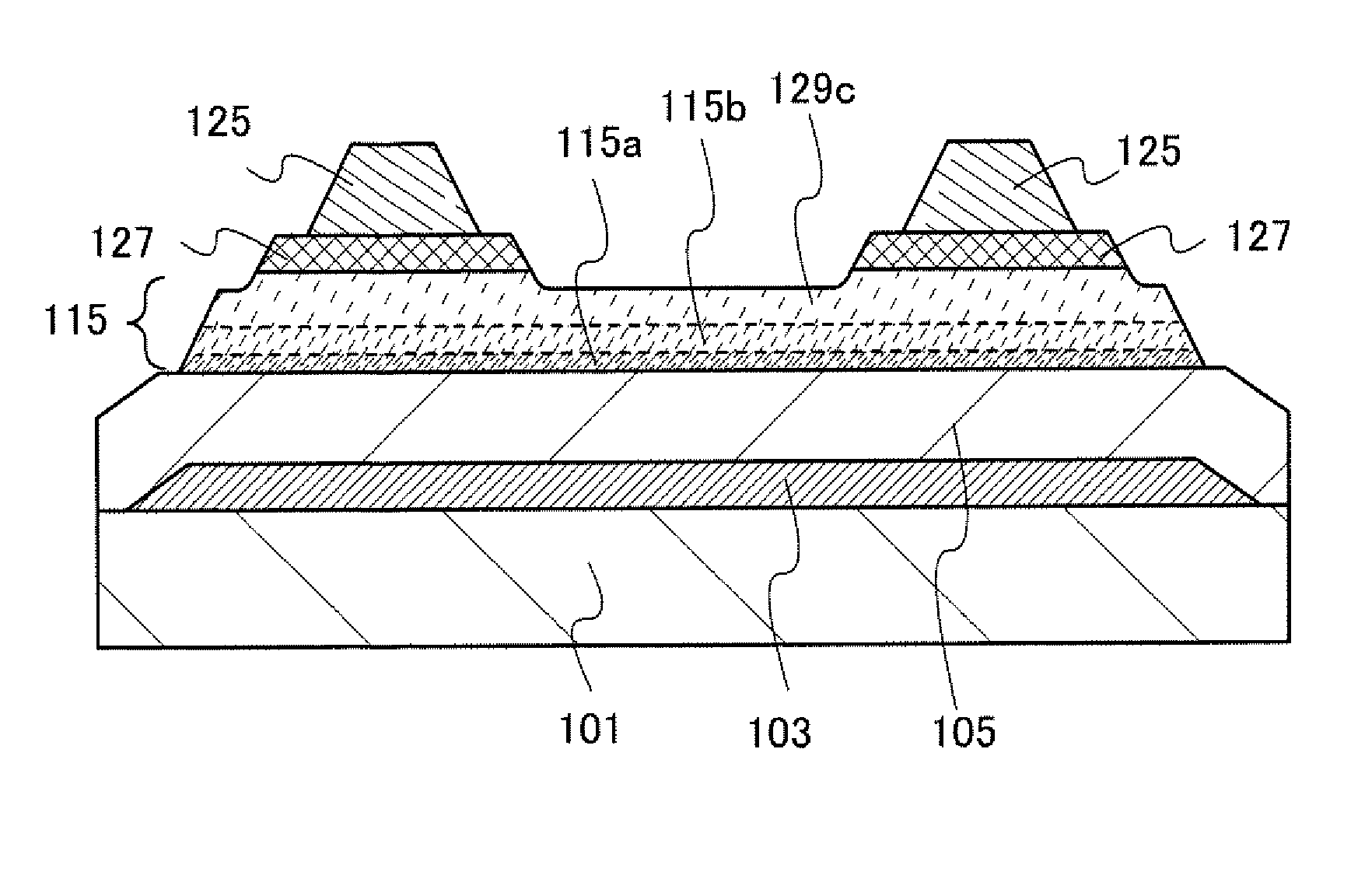
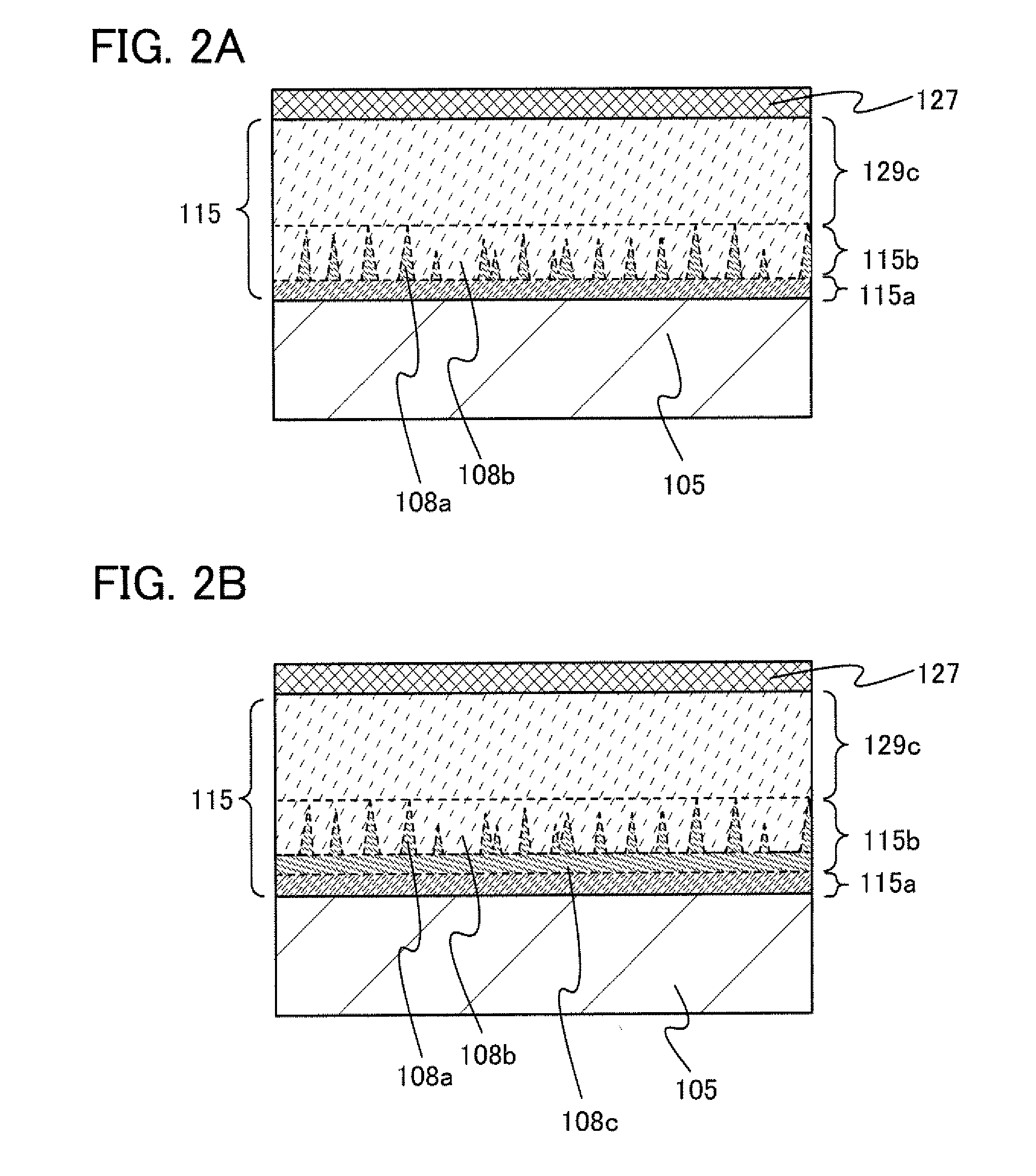
[0053]FIG. 1 is a cross-sectional view of an embodiment of a thin film transistor. The thin film transistor illustrated in FIG. 1 includes a gate electrode 103 over a substrate 101, a semiconductor layer 115 over a gate insulating layer 105, impurity semiconductor layers 127 serving as source and drain regions which are in contact with part of the upper surface of the semiconductor layer 115, and wirings 125 in contact with the impurity semiconductor layers 127. The semiconductor layer 115 includes a microcrystalline semiconductor layer 115a, a mixed layer 115b, and a layer 129c containing an amorphous semiconductor, which are stacked in sequence over the gate insulating layer 105.

[0054]As the substrate 101, a glass substrate, a ceramic substrate, a plastic substrate which has high heat resistance enough to withstand a process temperature of this manufacturing process, or the like can be used. In the case where the substrate does not need a light-transmitting property, a metal subst...

embodiment 2

[0124]In this embodiment, a method for manufacturing the thin film transistor described in Embodiment 1 will be described with reference to FIGS. 12A to 12C, FIGS. 13A to 13C, and FIGS. 14A-1 to 14B-2.

[0125]It is preferable that all thin film transistors formed over the same substrate have the same conductivity type because the number of manufacturing steps can be reduced. Therefore, in this embodiment, a method for manufacturing an n-channel thin film transistor is described.

[0126]First, a manufacturing process of the thin film transistor illustrated in FIG. 1 is described below.

[0127]As illustrated in FIG. 12A, a gate electrode 103 is formed over a substrate 101.

[0128]Then, a gate insulating layer 105 is formed so as to cover the gate electrode 103. After that, a first semiconductor layer 106 is formed.

[0129]The gate electrode 103 can be formed in such a manner that a conductive layer is formed over the substrate 101 using the material given in Embodiment 1 by a sputtering method ...

embodiment 3

[0176]In this embodiment, a method for manufacturing a thin film transistor, which is different from that in Embodiment 2, will be described with reference to FIGS. 12A to 12C, FIGS. 15A to 15C, and FIGS. 16A and 16B.

[0177]As in Embodiment 2, a gate electrode 103 is formed over a substrate 101. Then, a gate insulating layer 105 is formed so as to cover the gate electrode 103, and a first semiconductor layer 106 is formed (FIG. 12A). Next, as in Embodiment 2, crystals are grown from the first semiconductor layer 106, whereby a second semiconductor layer 107 (a mixed layer 107b and a layer 107c containing an amorphous semiconductor) is formed. Then, an impurity semiconductor layer 109 is formed over the second semiconductor layer 107 (FIG. 15A). After that, a resist mask (not illustrated) is formed over the impurity semiconductor layer 109.

[0178]Next, with the use of the resist mask, the second semiconductor layer 107 and the impurity semiconductor layer 109 are etched. By this step, ...


PUM


Abstract

A thin film transistor includes a gate insulating layer covering a gate electrode, a semiconductor layer in contact with the gate insulating layer, and impurity semiconductor layers which are in contact with part of the semiconductor layer and which form a source region and a drain region. The semiconductor layer includes a microcrystalline semiconductor layer formed on the gate insulating layer and a microcrystalline semiconductor region containing nitrogen in contact with the microcrystalline semiconductor layer. The thin film transistor in which off-current is small and on-current is large can be manufactured with high productivity.

Description

TECHNICAL HELD[0001]The present invention relates to a thin film transistor and a method for manufacturing the thin film transistor, and a display device to which the thin film transistor is applied.BACKGROUND ART[0002]As a kind of field-effect transistor, a thin film transistor in which a channel formation region is formed in a semiconductor layer fainted over a substrate having an insulating surface is known. Techniques for using amorphous silicon, microcrystalline silicon, and polycrystalline silicon for semiconductor layers in thin film transistors have been disclosed (see Patent Documents 1 to 5). A typical application of the thin film transistor is a liquid crystal television device in which the thin film transistor has been put to practical use as a switching transistor for a pixel that constitutes a display screen.REFERENCEPatent Document[Patent Document 1] Japanese Published Patent Application No. 2001-053283[0003][Patent Document 2] Japanese Published Patent Application No...

Claims


Application Information

Patent Timeline
Patent Type & Authority Applications(United States)
IPC IPC(8): H01L29/786
CPCH01L29/78678H01L29/78696H01L27/1288H01L51/52H01L29/78669H01L27/1214H01L29/04H01L29/06H10K50/80
Inventor MIYAIRI, HIDEKAZUWATABE, TAKEYOSHISHIMAZU, TAKASHI
Owner SEMICON ENERGY LAB CO LTD
Why Eureka
Try Eureka