Thin film transistor and display device including the same

a thin film transistor and display device technology, applied in the direction of optics, radio frequency controlled devices, instruments, etc., can solve the problems of reduced yield, increased cost, and complicated film production process, and achieve low resistance, increase the mobility of current and field effect, and reduce the effect of resistivity

Inactive Publication Date: 2009-07-02
SEMICON ENERGY LAB CO LTD
View PDF62 Cites 15 Cited by
  • Summary
  • Abstract
  • Description
  • Claims
  • Application Information

AI Technical Summary

Benefits of technology

[0024]According to the present invention, a semiconductor film with low resistivity containing germanium at a concentration greater than or equal to 5 at. % and less than or equal to 100 at. % or a conductive film with low resistivity is formed on a surface of an insulating film, an amorphous semiconductor film or an insulating film is formed, which covers a side surface of the semiconductor film containing germanium at a concentration greater than or equal to 5 at. % and less than or equal to 100 at. % or the conductive film, and a pair of wirings are formed over the amorphous semiconductor film or the insulating film, whereby increase of ON current and field effect mobility and improvement of electrical characteristics of the thin film transistor can be realized as well as reduction of off current of the thin film transistor. In addition, by manufacturing a display device including the thin film transistor, the image quality of the display device can be improved.

Problems solved by technology

However, the thin film transistor using a polycrystalline semiconductor film requires a more complicated process than the thin film transistor including an amorphous semiconductor film because of crystallization of the semiconductor film.
Thus, there are problems such as reduction in yield and increase in cost.
Further, an inverted staggered thin film transistor using a microcrystalline semiconductor film for a channel formation region has problems in that the crystallinity of an interface region between a gate insulating film and the microcrystalline semiconductor film is low and electric characteristics of the thin film transistor are poor.
A display device using thin film transistors having high off current has a problem in that contrast decreases and power consumption increases.

Method used


Image

  • Thin film transistor and display device including the same
  • Thin film transistor and display device including the same
  • Thin film transistor and display device including the same

Examples


embodiment mode 1

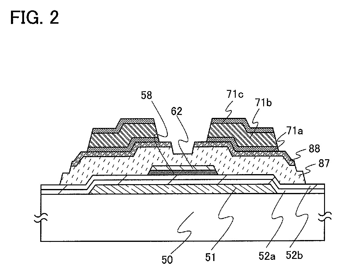
[0061]In this embodiment mode, a structure of a thin film transistor will be described, which has higher field effect mobility, a higher ON current, and a lower off current compared with a conventional thin film transistor including a microcrystalline semiconductor film in a channel formation region, with reference to FIGS. 1A and 1B, FIG. 2, FIG. 3, FIG. 4, FIG. 5, FIG. 6, FIG. 7, FIGS. 8A to 8C, FIGS. 9A to 9F, and FIGS. 35A and 35B.

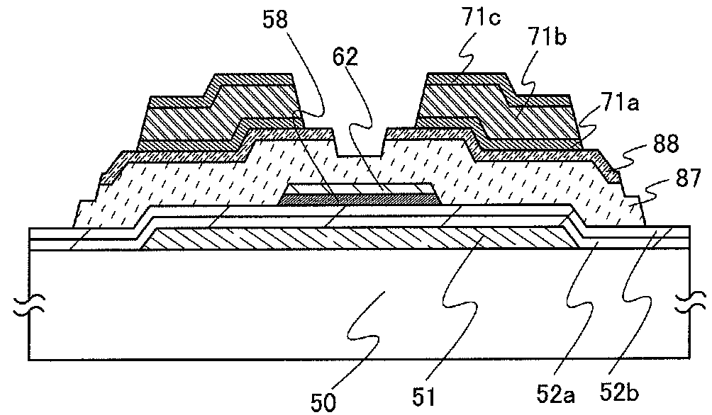
[0062]FIG. 1A illustrates a thin film transistor in which a gate electrode 51 is formed over a substrate 50, gate insulating films 52a and 52b are formed over the gate electrode 51, a semiconductor film 58 containing germanium at a concentration greater than or equal to 5 at. % and less than or equal to 100 at. % or a conductive film 58 is formed over the gate insulating films 52a and 52b, a buffer layer 42 is formed over the semiconductor film 58 containing germanium at a concentration greater than or equal to 5 at. % and less than or equal to 100 at....

embodiment mode 2

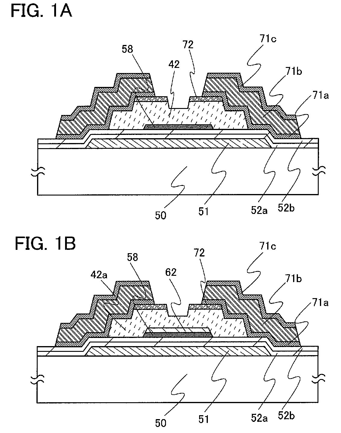
[0119]In this embodiment mode, another structure of the thin film transistor illustrated in Embodiment Mode 1 is described with reference to FIG. 1A and FIGS. 34A and 34B. Although FIG. 1A is referred to here, this embodiment mode can be applied to as appropriate to the thin film transistors illustrated in other drawings in Embodiment Mode 1.

[0120]In FIG. 1A, the end portion of the pair of source and drain regions 72 functioning as source and drain regions overlaps with the end portion of the semiconductor film 58 containing germanium at a concentration greater than or equal to 5 at. % and less than or equal to 100 at. % or the conductive film 58.

[0121]Further, in addition to the structure, as for the thin film transistor illustrated in FIG. 34A, when the end portion of the pair of source and drain regions 72 functioning as source and drain regions and the end portion of the semiconductor film 58 containing germanium at a concentration greater than or equal to 5 at. % and less than ...

embodiment mode 3

[0123]In this embodiment mode, a process for manufacturing a thin film transistor having high field effect mobility, high ON current, and low off current is described. Here, as a typical example, a method for manufacturing the thin film transistor of FIG. 1B in Embodiment Mode 1 is described.

[0124]An n-channel thin film transistor having an amorphous semiconductor film or a microcrystalline semiconductor film has higher field effect mobility than a p-channel thin film transistor having an amorphous semiconductor film or a microcrystalline semiconductor film and thus the n-channel thin film transistor is more suitable for being used in a driver circuit. It is preferable that all thin film transistors formed over one substrate have the same polarity in order to reduce the number of manufacturing steps. Further, when a semiconductor film containing germanium at a concentration greater than or equal to 5 at. % and less than or equal to 100 at. % is used for a semiconductor film 45 conta...


PUM

PropertyMeasurementUnit
crystal grain diameteraaaaaaaaaa
grain sizeaaaaaaaaaa
thicknessaaaaaaaaaa

Abstract

One object of the present invention is reduction of off current of a thin film transistor. Another object of the present invention is improvement of electric characteristics of the thin film transistor. Further, another object of the present invention is improvement of image quality of the display device including the thin film transistor. The thin film transistor includes a semiconductor film containing germanium at a concentration greater than or equal to 5 at. % and less than or equal to 100 at. % or a conductive film which is provided over a gate electrode with the gate insulating film interposed therebetween and which is provided in an inner region of the gate electrode so as not to overlap with an end portion of the gate electrode, a film covering at least a side surface of the semiconductor film containing germanium at a concentration greater than or equal to 5 at. % and less than or equal to 100 at. % or the conductive film, a pair of wirings formed over the film covering the side surface of the semiconductor film containing germanium at a concentration greater than or equal to 5 at. % and less than or equal to 100 at. % or the conductive film.

Description

BACKGROUND OF THE INVENTION[0001]1. Field of the Invention[0002]The present invention relates to a thin film transistor and a display device using the thin film transistor at least in a pixel portion.[0003]2. Description of the Related Art[0004]In recent years, techniques for forming a thin film transistor using a semiconductor thin film (with a thickness of about several tens to several hundreds of nanometers) which is formed over a substrate having an insulating surface have attracted attention. A thin film transistor is widely used in an electronic device such as ICs and electro-optical devices, and their development especially as a switching element for a display device has been accelerated.[0005]As a switching element of a display device, a thin film transistor using an amorphous semiconductor film for a channel formation region, a thin film transistor using a polycrystalline semiconductor film with a crystal grain diameter of 100 nm or more for a channel formation region, or t...

Claims


Application Information

Patent Timeline
Patent Type & Authority Applications(United States)
IPC IPC(8): H01L29/786H01L33/00G02F1/1368H01L51/50
CPCH01L27/1214H01L29/458H01L27/1288H01L29/78684H01L29/78696H01L29/4908
Inventor YAMAZAKI, SHUNPEI
Owner SEMICON ENERGY LAB CO LTD
Why Eureka
Try Eureka