Method for manufacturing thin film transistor

a thin film transistor and display device technology, applied in the direction of coatings, solid-state devices, chemical vapor deposition coatings, etc., can solve the problems of high manufacturing cost, inability to obtain sufficient switching characteristics, and low field-effect mobility and small on-current, so as to increase the active species amount, increase the deposition rate of the first semiconductor layer, and promote the reaction between active species

Inactive Publication Date: 2010-05-20
SEMICON ENERGY LAB CO LTD
View PDF53 Cites 15 Cited by
  • Summary
  • Abstract
  • Description
  • Claims
  • Application Information

AI Technical Summary

Benefits of technology

[0016]As a source gas of the first semiconductor layer, a rare gas such as helium, argon, neon, krypton, or xenon is used, whereby plasma is stabilized, dissociation of the deposition gas containing silicon or germanium and hydrogen is promoted, and the amount of active species is increased. Therefore, reaction between the active species is promoted and the deposition rate of the first semiconductor layer is increased. Further, as the deposition rate is increased, the deposition time of the first semiconductor layer becomes short and the amount of impurities taken in a treatment chamber during deposition is reduced. Therefore, the amount of impurities included in the first semiconductor layer is reduced, whereby crystallinity of the first semiconductor layer is increased. Accordingly, on-current and field-effect mobility of the thin film transistor can be increased.
[0017]Further, a gas containing nitrogen such as ammonia, nitrogen, nitrogen fluoride, or nitrogen chloride is used to form the second semiconductor layer together with the deposition gas containing silicon or germanium and hydrogen, whereby the layer including a microcrystalline semiconductor and an amorphous semiconductor, which includes a plurality of conical or pyramidal projections formed of a microcrystalline semiconductor, can be formed. Furthermore, an amorphous semiconductor layer containing nitrogen may be formed on the layer including a microcrystalline semiconductor and an amorphous semiconductor. Therefore, regions in contact with source and drain regions and a back channel side are each formed using an amorphous semiconductor layer with high resistance, whereas between the channel formation region and the source and drain regions, a plurality of conical or pyramidal projections is formed of the microcrystalline semiconductor which has low resistance, so that off-current can be reduced, and further, on-current is increased by reducing resistance between the source and drain regions and the channel formation region. In addition, the threshold voltage can be controlled with the use of a gas containing nitrogen as the source gas of the second semiconductor layer.
[0018]Note that a rare gas such as helium, argon, neon, krypton, or xenon, is used as the source gas of the second semiconductor layer, so that the deposition rate can be increased.
[0019]Accordingly, a thin film transistor in which off-current is small, on-current is large, and the threshold voltage is controlled can be manufactured with high productivity.

Problems solved by technology

A thin film transistor in which a channel is formed using an amorphous silicon layer has problems such as low field-effect mobility and small on-current.
On the other hand, a thin film transistor in which a channel is formed using a microcrystalline silicon layer has a problem in that, whereas the field-effect mobility is higher than that of the thin film transistor in which a channel is formed using an amorphous silicon layer, the off-current is large, and thus sufficient switching characteristics cannot be obtained.
However, a thin film transistor formed using a polycrystalline silicon layer requires a crystallization process of a semiconductor layer and has a problem of higher manufacturing cost as compared to a thin film transistor formed using an amorphous silicon layer.
For example, with the laser annealing technique involved in the process of manufacturing a polycrystalline silicon layer, large-screen liquid crystal panels cannot be produced efficiently because the irradiation area of a laser beam is small.

Method used


Image

  • Method for manufacturing thin film transistor
  • Method for manufacturing thin film transistor
  • Method for manufacturing thin film transistor

Examples


embodiment 1

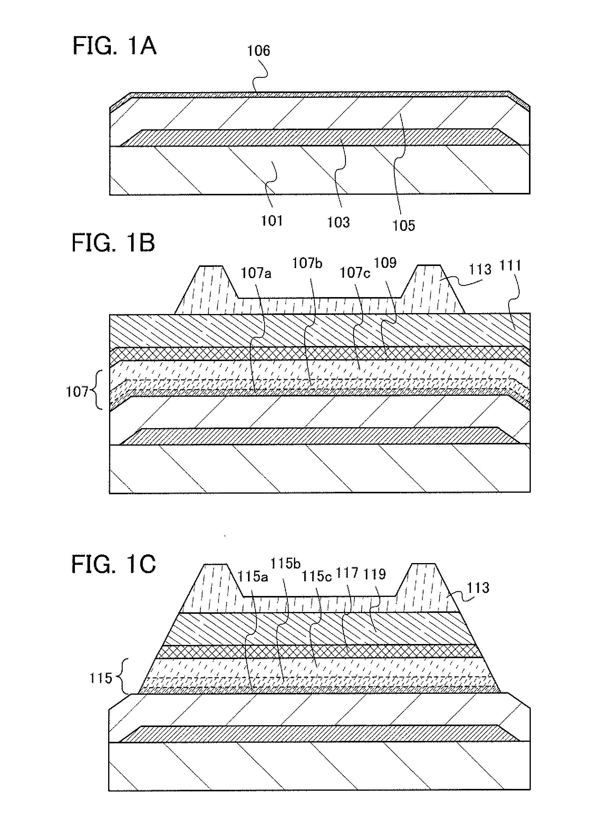
[0042]In Embodiment 1, a method for manufacturing a thin film transistor is described with reference to FIGS. 1A to 1C, FIGS. 2A and 2B, FIG. 3, FIGS. 4A1, 4A2, 4B1, and 4B2, FIGS. 5A to 5C, FIG. 6, FIG. 7, FIG. 8, and FIG. 9. An n-channel thin film transistor has higher carrier mobility than a p-channel thin film transistor. In addition, it is preferable that all thin film transistors formed over the same substrate have the same conductivity to reduce the number of manufacturing steps. Therefore, in Embodiment 1, a method for manufacturing an n-channel thin film transistor is described.

[0043]A gate electrode 103 is formed over a substrate 101. Then, a gate insulating layer 105 is formed so as to cover the gate electrode 103. A first semiconductor layer 106 is formed over the gate insulating layer 105 (see FIG. 1A).

[0044]As the substrate 101, a glass substrate, a ceramic substrate, a plastic substrate which has high heat resistance enough to withstand a process temperature of this m...

embodiment 2

[0126]In Embodiment 2, one embodiment of a plasma CVD apparatus which can be used for forming the gate insulating layer 105, the first semiconductor layer 106, the second semiconductor layer 107, and the impurity semiconductor layer 109 is described in detail. These layers are formed by a CVD method or the like.

[0127]A plasma CVD apparatus 261 illustrated in FIG. 6 is connected to a gas supply means 250 and an exhaust means 251.

[0128]The plasma CVD apparatus 261 illustrated in FIG. 6 includes a treatment chamber 241, a stage 242, a gas supply portion 243, a shower plate 244, an exhaust port 245, an upper electrode 246, a lower electrode 247, an alternate-current power source 248, and a temperature control portion 249.

[0129]The treatment chamber 241 is formed using a material having rigidity and the inside thereof can be evacuated to vacuum. The treatment chamber 241 is provided with the upper electrode 246 and the lower electrode 247. Note that in FIG. 6, a structure of a capacitive...

embodiment 3

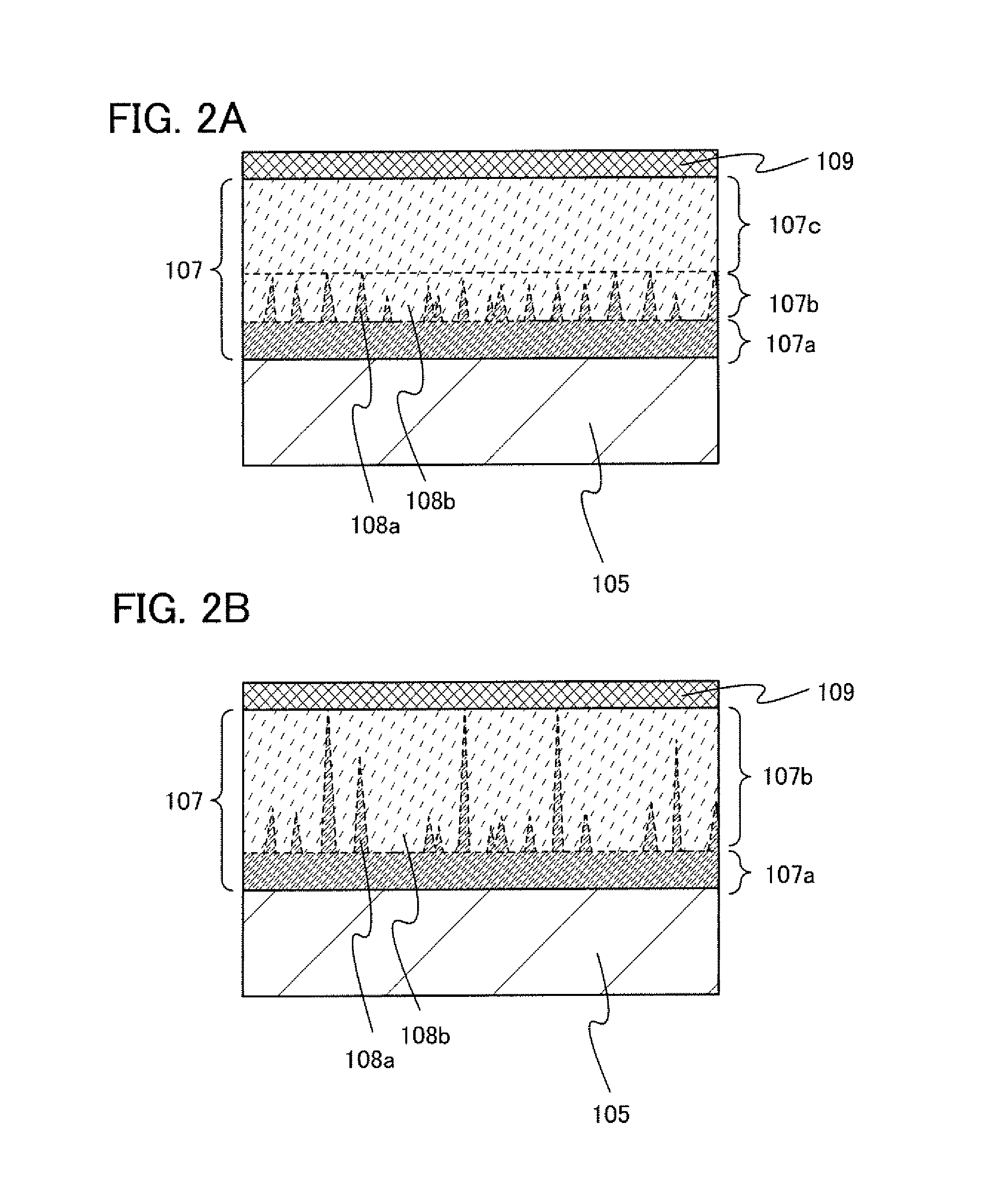
[0135]In Embodiment 3, a process of forming a second semiconductor layer 107 which can be applied to Embodiment 1 are described.

[0136]In Embodiment 3, the inside of a treatment chamber is cleaned before the second semiconductor layer 107 is formed, and after that, the inner wall of the chamber is covered with a silicon nitride layer, whereby nitrogen is included in the second semiconductor layer 107, the oxygen concentration is made low, and the nitrogen concentration is made higher than the oxygen concentration. A series of steps from a step of forming the gate insulating layer 105 to a step of forming the first semiconductor layer 106 is similar to that in Embodiment 1; thus, a series of steps from a step of forming a second semiconductor layer 107 to a step of forming an impurity semiconductor layer 109 is described below with reference to FIG. 7.

[0137]The first semiconductor layer 106 is formed over the entire surface of the gate insulating layer 105. First, the source gases use...


PUM

PropertyMeasurementUnit
sizeaaaaaaaaaa
sizeaaaaaaaaaa
sizeaaaaaaaaaa

Abstract

An object is to provide a method for manufacturing a thin film transistor having favorable electric characteristics, with high productivity. A gate electrode is formed over a substrate and a gate insulating layer is formed over the gate electrode. A first semiconductor layer is formed over the gate insulating layer by generating plasma using a deposition gas containing silicon or germanium, hydrogen, and a rare gas. Next, a second semiconductor layer including an amorphous semiconductor and a microcrystal semiconductor is formed in such a manner that the first semiconductor layer is partially grown as a seed crystal by generating plasma using a deposition gas containing silicon or germanium, hydrogen, and a gas containing nitrogen. Then, a semiconductor layer to which an impurity imparting one conductivity is added is formed and a conductive film is formed. Thus, a thin film transistor is manufactured.

Description

BACKGROUND OF THE INVENTION[0001]1. Field of the Invention[0002]The present invention relates to a method for manufacturing a thin film transistor and a display device to which the thin film transistor is applied.[0003]2. Description of the Related Art[0004]As a kind of field-effect transistor, a thin film transistor in which a channel region is formed in a semiconductor layer formed over a substrate having an insulating surface is known. Techniques for using amorphous silicon, microcrystalline silicon, and polycrystalline silicon for semiconductor layers in thin film transistors have been disclosed (see Patent Documents 1 to 5). A typical application of thin film transistors is a liquid crystal television device, in which thin film transistors have been put to practical use as a switching transistor for each pixel that constitutes a display screen.[Patent Documents][Patent Document 1] Japanese Published Patent Application No. 2001-053283[Patent Document 2] Japanese Published Patent...

Claims


Application Information

Patent Timeline
Patent Type & Authority Applications(United States)
IPC IPC(8): H01L21/336
CPCC23C16/0272C23C16/24C23C16/50H01L27/1288H01L29/66765H01L29/78669H01L29/78678H01L27/1214
Inventor TAKAHASHI, ERIKAKATO, TAKAYUKIMIYAIRI, HIDEKAZUJINBO, YASUHIROICHIJO, MITSUHIROYOKOI, TOMOKAZU
Owner SEMICON ENERGY LAB CO LTD
Why Eureka
Try Eureka