Fluorine depleted adhesion layer for metal interconnect structure

a metal interconnect and fluorine depletion technology, applied in the field of metal interconnect structure, can solve the problems of disadvantageous effect on reliability of a semiconductor package employing lead-free c4 balls, and achieve the effect of improving adhesion

Active Publication Date: 2009-08-27
TAIWAN SEMICON MFG CO LTD
View PDF3 Cites 19 Cited by
  • Summary
  • Abstract
  • Description
  • Claims
  • Application Information

AI Technical Summary

Benefits of technology

[0007]The present invention addresses the needs described above by providing a metal interconnect structure in which a fluorine-depleted adhesion layer is located between a metal line and a fluorosilicate glass (FSG) layer to provide an enhanced adhesion between the metal line and the FSG layer.

Problems solved by technology

This has a disadvantageous effect on reliability of a semiconductor package employing lead-free C4 balls.

Method used


Image

  • Fluorine depleted adhesion layer for metal interconnect structure
  • Fluorine depleted adhesion layer for metal interconnect structure
  • Fluorine depleted adhesion layer for metal interconnect structure

Examples


Embodiment Construction

[0058]As stated above, the present invention relates to a metal interconnect structure employing a fluorine depleted adhesion layer and methods of manufacturing the same, which are now described in detail with accompanying figures.

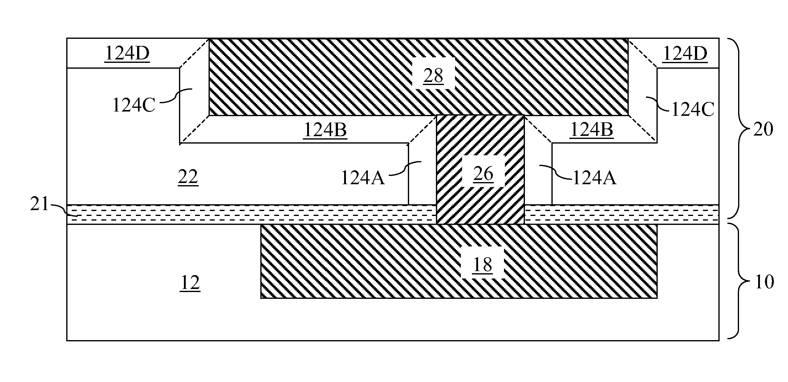
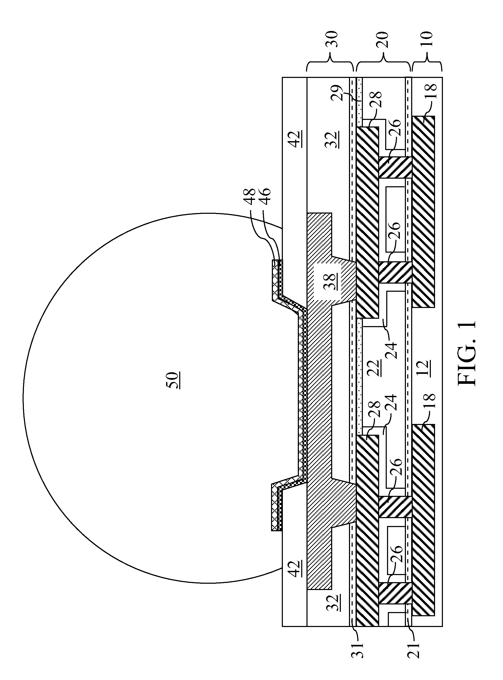
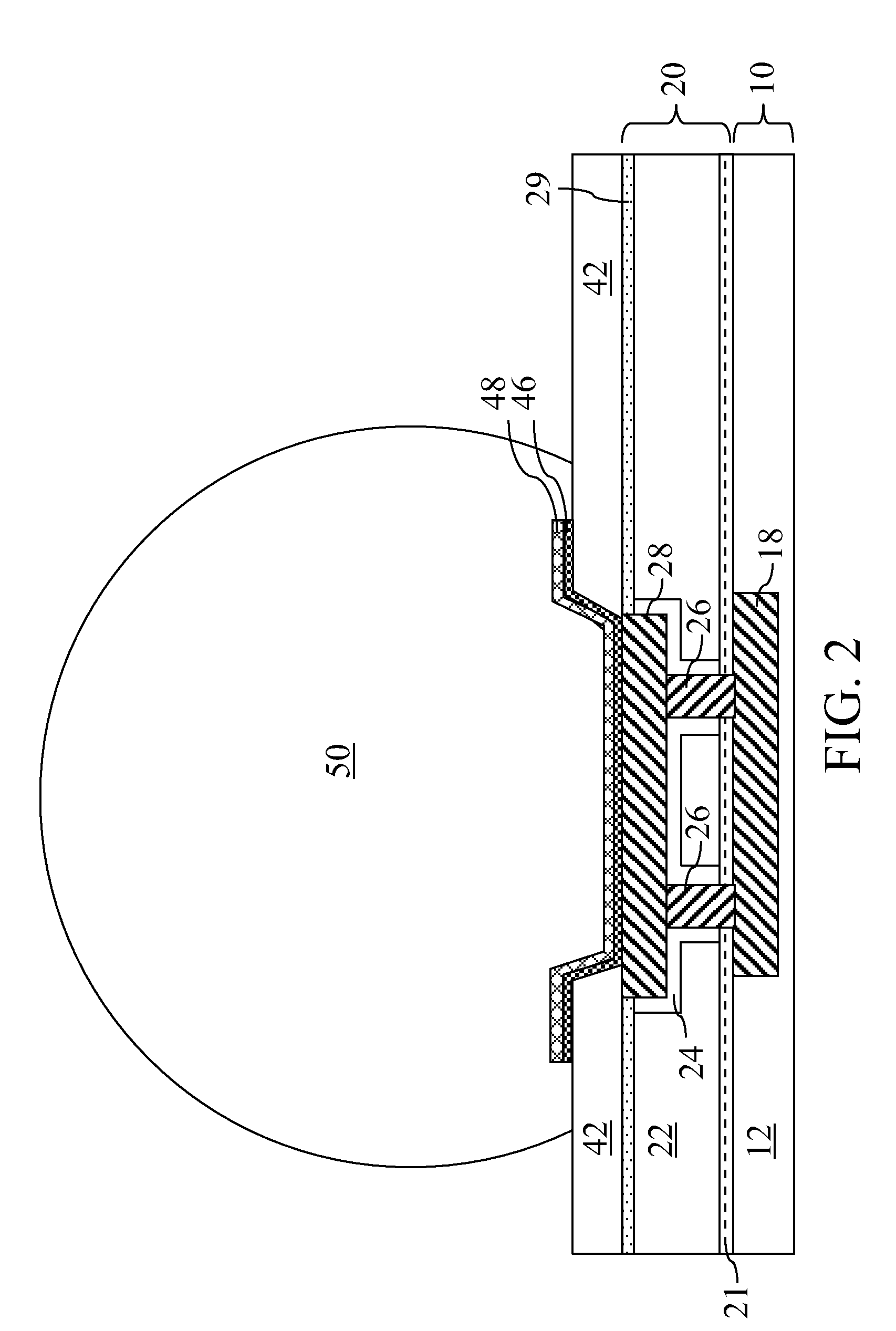
[0059]Referring to FIG. 1, an exemplary structure comprising a C4 ball and a metal interconnect structure incorporating features of the present invention is shown. The exemplary structure comprises an underlying interconnect level 10, a final interconnect level 20, a metal pad level 30, a dielectric passivation layer 42, a metallic adhesion layer 46, a wetting layer 48, and a lead-free C4 ball 50 that are formed on a semiconductor substrate (not shown). Semiconductor devices (not shown) are formed on the semiconductor substrate by employing semiconductor manufacturing processes known in the art. Typically, additional BEOL interconnect structures (not shown) are present between the semiconductor devices and the underlying interconnect level 10. The addition...


PUM

PropertyMeasurementUnit
dielectric constantaaaaaaaaaa
thicknessaaaaaaaaaa

Abstract

A line trough and a via cavity are formed within a dielectric layer comprising a fluorosilicate glass (FSG) layer. A fluorine depleted adhesion layer is formed within the line trough and the via cavity either by a plasma treatment that removes fluorine from exposed surfaces of the FSG layer, or by deposition of a substantially fluorine-free dielectric layer. Metal is deposited within the line trough and the via cavity to form a metal line and a metal via. The fluorine depleted adhesion layer provides enhanced adhesion to the metal line compared with prior art structures in which a metal line directly contacts a FSG layer. The enhanced adhesion of metal with an underlying dielectric layer provides higher resistance to delamination for a semiconductor package employing lead-free C4 balls on a metal interconnect structure.

Description

FIELD OF THE INVENTION[0001]The present invention relates to a semiconductor structure, and particularly to a metal interconnect structure employing a fluorine depleted layer for improved adhesion and methods of manufacturing the same.BACKGROUND OF THE INVENTION[0002]Once formation of semiconductor devices and interconnects on a semiconductor wafer (substrate) is completed, the semiconductor wafer is diced into semiconductor chips, or “dies.” Functional semiconductor chips are then packaged to facilitate mounting on a circuit board. A package is a supporting element for the semiconductor chip that provides mechanical protection and electrical connection to an upper level assembly system such as the circuit board. One typical packaging technology is Controlled Collapse Chip Connection (C4) packaging, which employs C4 balls each of which contacts a C4 pad on the semiconductor chip and another C4 pad on a packaging substrate. The packaging substrate may then be assembled on the circuit...

Claims


Application Information

Patent Timeline
Patent Type & Authority Applications(United States)
IPC IPC(8): H01L21/768H01L23/522
CPCH01L21/76807H01L21/76814H01L21/76826H01L21/76829H01L23/53295H01L23/5226H01L23/53238H01L23/5329H01L21/76831H01L24/03H01L24/05H01L24/06H01L24/13H01L2224/0401H01L2224/05001H01L2224/05022H01L2224/05027H01L2224/05124H01L2224/05147H01L2224/05166H01L2224/05181H01L2224/05572H01L2224/05639H01L2224/05644H01L2224/05666H01L2224/11H01L2224/13006H01L2924/0002H01L2924/00014H01L2924/00
Inventor FAROOQ, MUKTA G.KINSER, EMILY R.
Owner TAIWAN SEMICON MFG CO LTD
Why Eureka
Try Eureka