Needle trace transfer member and probe apparatus

a technology of transfer member and needle trace, which is applied in the direction of measuring device, semiconductor/solid-state device testing/measurement, instruments, etc., can solve the problems of inability to avoid variations in manufacturing process, inability to accurately align the target and the probe card, and inability to eliminate the variation of production quality of the probe card. , to achieve the effect of suppressing the effect of the temperature of the needle trace transfer member and eliminating the needle trace in a short period of tim

Active Publication Date: 2009-08-27
TOKYO ELECTRON LTD
View PDF8 Cites 67 Cited by
  • Summary
  • Abstract
  • Description
  • Claims
  • Application Information

AI Technical Summary

Benefits of technology

[0007]In view of the above, the present invention provides a needle trace transfer member which is capable of improving a throughput of inspection by eliminating needle traces in a short period of time and also capable of suppressing an effect of a temperature of the needle trace transfer member during high-temperature inspection, and a probe apparatus provided with the needle trace transferring member.

Problems solved by technology

As a result, considerable time is spent to align the target and the probe card.
Further, the probe card is not free from variations in production quality or the like, and even if the probe cards are of the same specification, the variations are hardly avoidable in the manufacturing process.
However, huge costs are incurred in developing such dedicated algorithms.
Therefore, the needle traces may be eliminated during the inspection performed at a high temperature above 100° C. Accordingly, it is difficult to use this method in the high temperature inspection.
Even if this method is used, since the temperature of the transfer sheet is considerably lower than that of the mounting table, the large temperature difference between the transfer sheet and the mounting table may adversely affect the high-temperature inspection.

Method used


Image

  • Needle trace transfer member and probe apparatus
  • Needle trace transfer member and probe apparatus
  • Needle trace transfer member and probe apparatus

Examples


Embodiment Construction

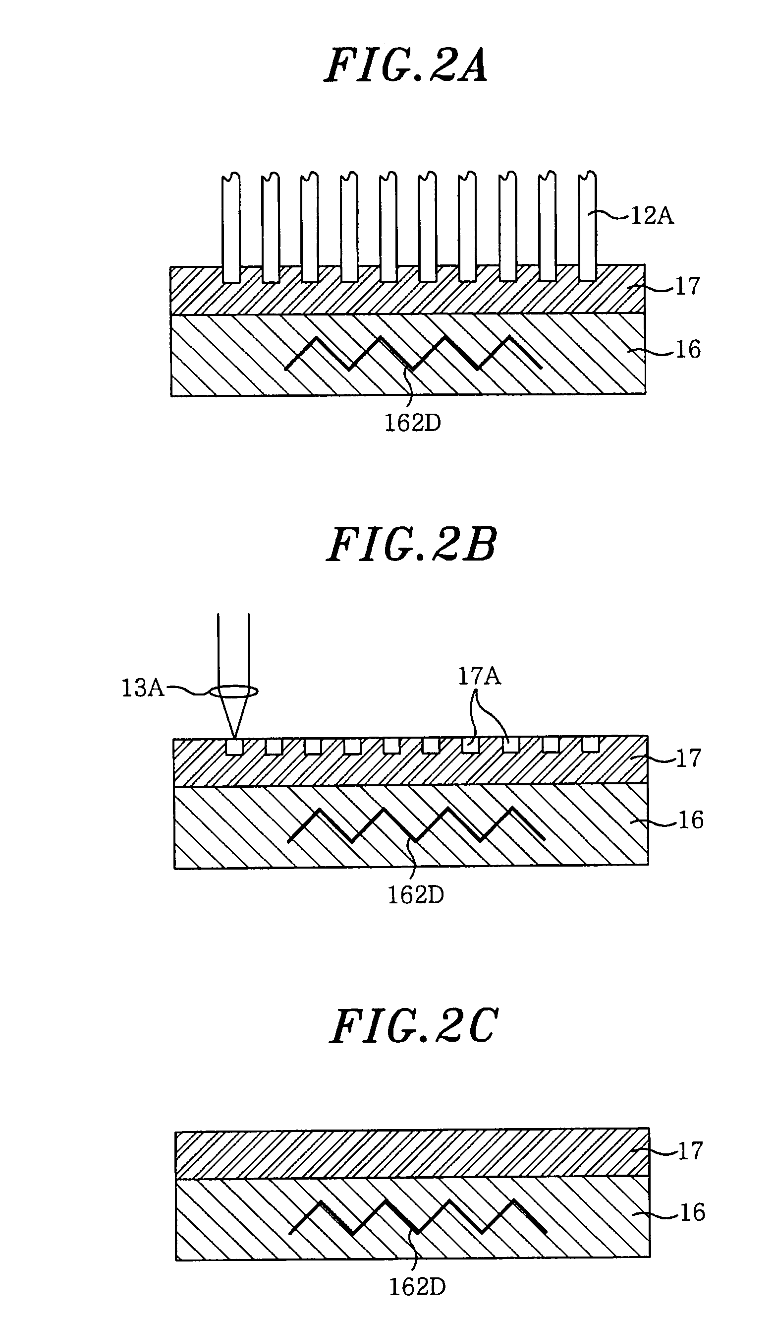
[0023]Hereinafter, an embodiment of the present invention will be described with reference to FIGS. 1 to 7.

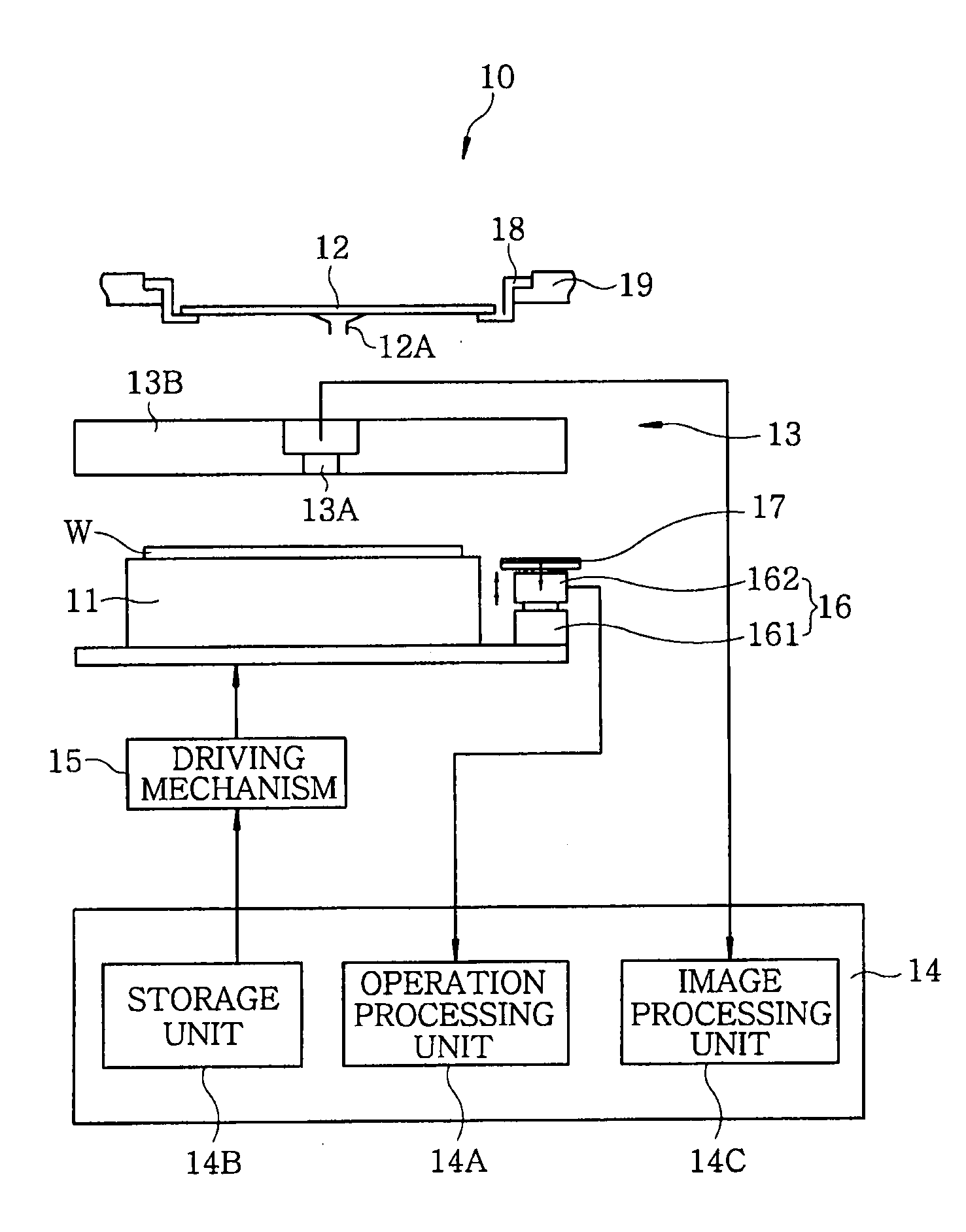
[0024]Above all, a probe apparatus of the present embodiment will be described with reference to, e.g., FIG. 1. As shown in FIG. 1, the probe apparatus 10 of the present embodiment includes a movable wafer chuck 11 for mounting thereon a target object(semiconductor wafer) W, a probe card 12 arranged above the wafer chuck 11, an alignment mechanism 13 for aligning a plurality of probes 12A of the probe card 12 with the semiconductor wafer W mounted on the wafer chuck 11, and a control unit 14 for controlling the wafer chuck 11, the alignment mechanism 13 and the like. Under the control of the control unit 14, the alignment mechanism 13 is driven to align the semiconductor wafer W mounted on the wafer chuck 11 and the probes 12A of the probe card 12. Subsequently, the electrical characteristics inspection of the semiconductor wafer W are conducted by brining the probes 12A into e...


PUM


Abstract

A needle trace transfer member to which needle traces of probes are transferred is installed at a movable mounting table to align the probes before electrical characteristics of a target object on the mounting table are inspected by bringing the probes into electrical contact with the target object. The needle trace transfer member is made of a shape memory polymer transformed reversibly and rapidly between a glass state with a high modulus elasticity and a rubber state with a low modulus of elasticity near its glass transition temperature. The glass transition temperature is set to a temperature close to a set temperature of the mounting table. The shape memory polymer is mainly made of polyurethane-based resin.

Description

FIELD OF THE INVENTION[0001]The present invention relates to a member to which needle traces of probes are transferred (hereinafter, referred to as “needle trace transfer member”) and a probe apparatus; and, more particularly, to a needle trace transfer member to which needle traces of probes are transferred to align the probes, and a probe apparatus having the needle trace transfer member when inspecting electrical characteristics of a target object by contacting the probes with the objectBACKGROUND OF THE INVENTION[0002]When electrical characteristics of a target object such as a semiconductor wafer or the like are inspected by using a plurality of probes, the electrical characteristic inspection is performed by, e.g., imaging tips of the probes provided at a probe card by a camera, detecting tip positions of the probes and contacting the probes with electrode pads of the target object. When the tip positions of the probes are detected by using a camera, time is required to focus ...

Claims


Application Information

Patent Timeline
Patent Type & Authority Applications(United States)
IPC IPC(8): G01R31/02
CPCG01R1/07364G01R31/2891G01R3/00H01L22/00
Inventor YAMADA, HIROSHIKATAGIRI, HIROFUMIWATANABE, TETSUJIKAWAJI, TAKESHI
Owner TOKYO ELECTRON LTD
Why Eureka
Try Eureka