

Stacked memory and fuse chip
- Summary
- Abstract
- Description
- Claims
- Application Information
AI Technical Summary
Benefits of technology
Problems solved by technology
Method used
Image

Examples
first embodiment
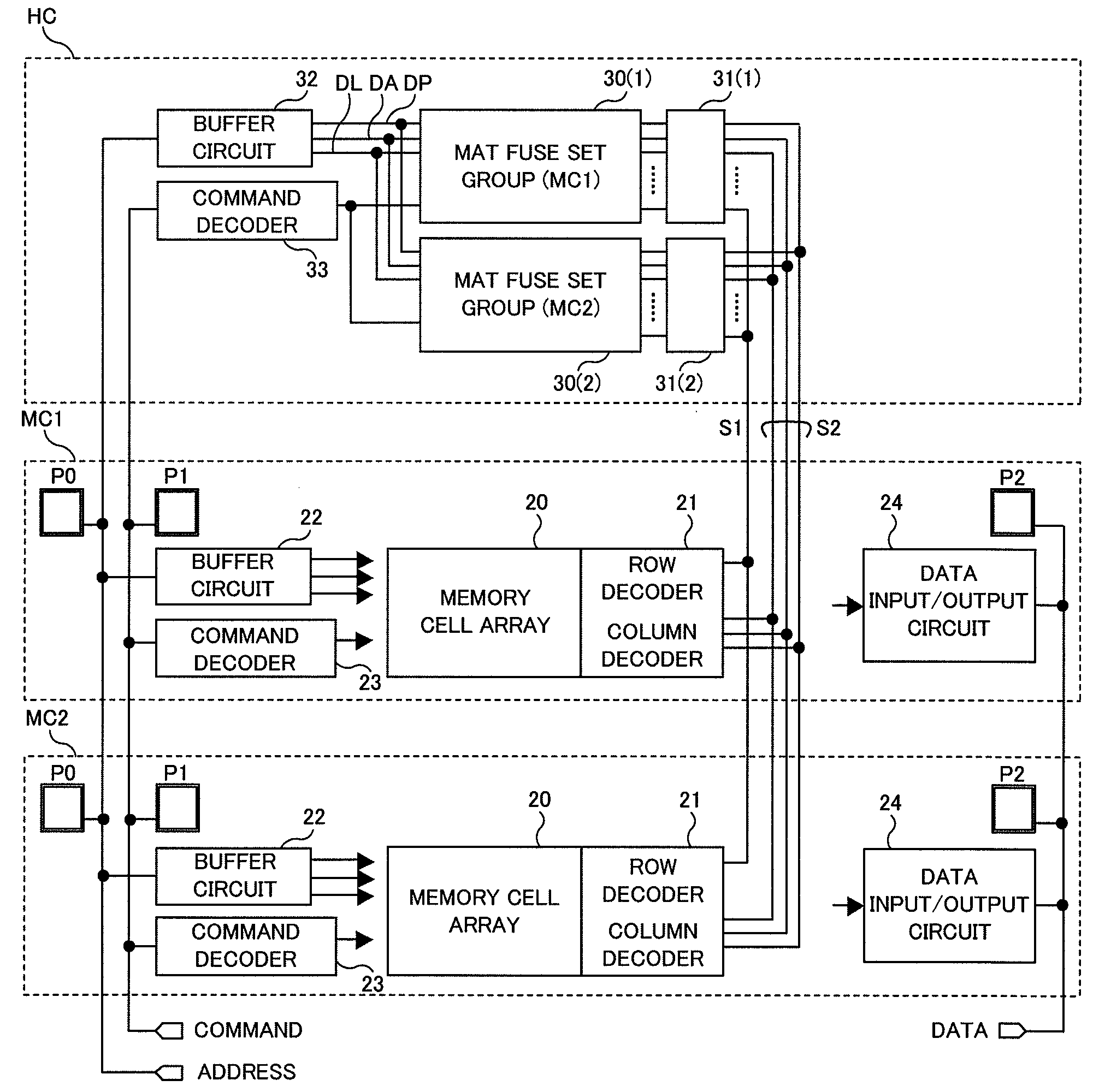
[0031]A stacked memory of the first embodiment is configured to have a plurality of memory core chips functioning as the DRAM chips and a fuse chip. FIG. 1 shows a planar structure of a memory core chip MC of the stacked memory, and FIG. 2 shows a planar structure of a fuse chip HC of the stacked memory. The memory core chip MC shown in FIG. 1 has a memory cell array area R1 divided into a plurality of areas, and has a through electrode area R2 and a test pad area R3 which are arranged between areas of the memory cell array area R. Each of four unit areas into which the memory cell array area R1 is divided forms a mat, and each mat includes the same number of memory cells. A large number of through electrodes for mutually connecting between chips of the stacked memory in a stacking direction are formed in the through electrode area R2. A large number of test pads used in a test of the memory core chips MC are formed in the test pad area R3.
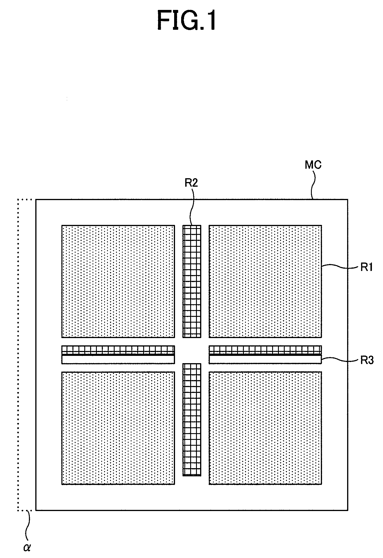
[0032]Meanwhile, the fuse chip HC shown in ...
second embodiment
[0061]A stacked memory of the second embodiment is based on the stacked memory of the first embodiment and is characterized that wafer stacking technique is applied thereto. In the stacked memory of the second embodiment, FIG. 7 shows a planar structure of the memory core chip MC, and FIG. 8 shows a planar structure of the fuse chip HC. The memory core chip MC shown in FIG. 7 has the memory cell array area R1 divided into a plurality of areas, and has the through electrode area R2 which are arranged between areas of the memory cell array area R1. Meanwhile, the fuse chip HC of FIG. 8 has a test pad area R12 in addition to the fuse area R10 and the through electrode area R11. Accordingly, when comparing FIGS. 7 and 8 with FIGS. 1 and 2 of the first embodiment, it is understood that the test pad area R3 (FIG. 1) is not provided on the memory core chip MC and the test pad area R12 is provided on the fuse chip HC. In addition, functions of the respective areas in FIGS. 7 and 8 are the s...
PUM
 Abstract
Description
Claims
Application Information