Laser-based technique for the transfer and embedding of electronic components and devices

a technology of electronic components and lasers, applied in the direction of transfer patterning, lithography/patterning, printed circuit aspects, etc., can solve the problems of inherently limited approaches, no techniques capable of transferring, mounting and interconnecting unpackaged semiconductor devices (baredies) onto circuit boards or other types of substrates, and limit the level of miniaturization that can be achieved

Active Publication Date: 2009-09-03
USA AS REPRESENTED BY THE SEC OF THE NAVY THE
View PDF14 Cites 71 Cited by
  • Summary
  • Abstract
  • Description
  • Claims
  • Application Information

AI Technical Summary

Benefits of technology

[0010]A method for transferring a component to a substrate comprising providing a laser; providing a receiving substrate; providing a carrier substrate comprising a laser-transparent support having a back surface and a front surface, wherein the front surface is in connection with a polymer material, wherein said polymer material is in connection with at least one transfer component, said transfer component comprising an active side and an inactive side, wherein said active side is in connection with said polymer material, wherein the polymer material has the property of being or becoming more volatile than the transfer component when exposed to laser energy; positioning the laser in relation to the carrier substrate and exposing the carrier substrate to laser energy from the laser so that the laser energy is directed through the back surface of the carrier substrate and through the laser-transparent support to strike the polymer material at a defined carrier location with sufficient energy to volatilize the polymer material at the location, causing the transfer component to desorb from the location and be lifted from the surface of the support; and positioning the receiving substrate in a spaced relation to the carrier substrate so that the at least one component of the transfer material is deposited at a defined receiving location on the receiving substrate, wherein said inactive side of said component is in connection with said receiving substrate.

Problems solved by technology

The resulting assembly on a printed circuit board is rather bulky compared with the bare-die itself and thus limits the level of miniaturization that can be achieved in a circuit requiring several packaged semiconductor devices and associated passive components.
Currently there are no techniques capable of transferring, mounting and interconnecting unpackaged semiconductor devices (bare-dies) onto circuit boards or other types of substrates.
Techniques for embedding passive components such as resistors and capacitors have been developed to address miniaturization goals, albeit partially, since they are not capable of embedding active components.
Such approaches are inherently limited as they require development of each individual circuit design. require significant volume for the final circuit design, do not allow the fabrication of truly embedded circuits, reduce the ability to add additional components or modify designs to circuits and are not compatible with active components such as transistors, LED's and integrated circuits.
As the demand for miniaturization has grown, however, the size of these packaged components has become a limiting factor.
However, development of these single-chip designs is costly and time-consuming, and once the chips are completed, their designs are very difficult to change.
Embedding passive components, such as resistors and capacitors, inside a circuit board is not a new technology.
However, embedding active semiconductor components has been demonstrated only in specialized applications because the bare semiconductor die are very fragile and tend to be damaged easily by the robotic systems (called “pick-and-place” tools) that mount the devices on a circuit board.
Furthermore, pick-and-place tools are ineffective at handling small (less than 1 mm square) or extremely thin (less than 50 μm thick) die, and they are unsuitable also for high-throughput applications (more than 10 devices per second).
Despite the success obtained with MEMS structures, this group did not attempt the application of this process to the transfer of functional semiconductor bare die.
However, in this technique, the devices are never transferred across a gap.
However, the authors did not discuss whether or not the dies were damaged after the transfer.
Furthermore, this configuration is not very practical for embedding individual devices, due to the difficulties in establishing the electrical connections to the pads on the patterned side of the die, which end up facing the bottom of the pocket in which the device has been embedded.
The challenge, however, is to be able to illuminate the active region of the die with the laser release / transfer pulse without damaging it.

Method used


Image

  • Laser-based technique for the transfer and embedding of electronic components and devices
  • Laser-based technique for the transfer and embedding of electronic components and devices
  • Laser-based technique for the transfer and embedding of electronic components and devices

Examples


Embodiment Construction

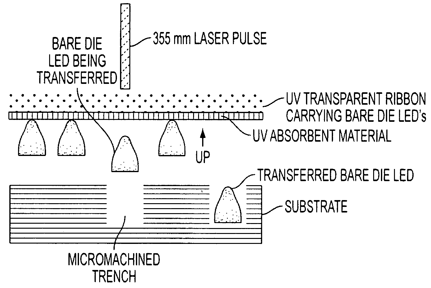
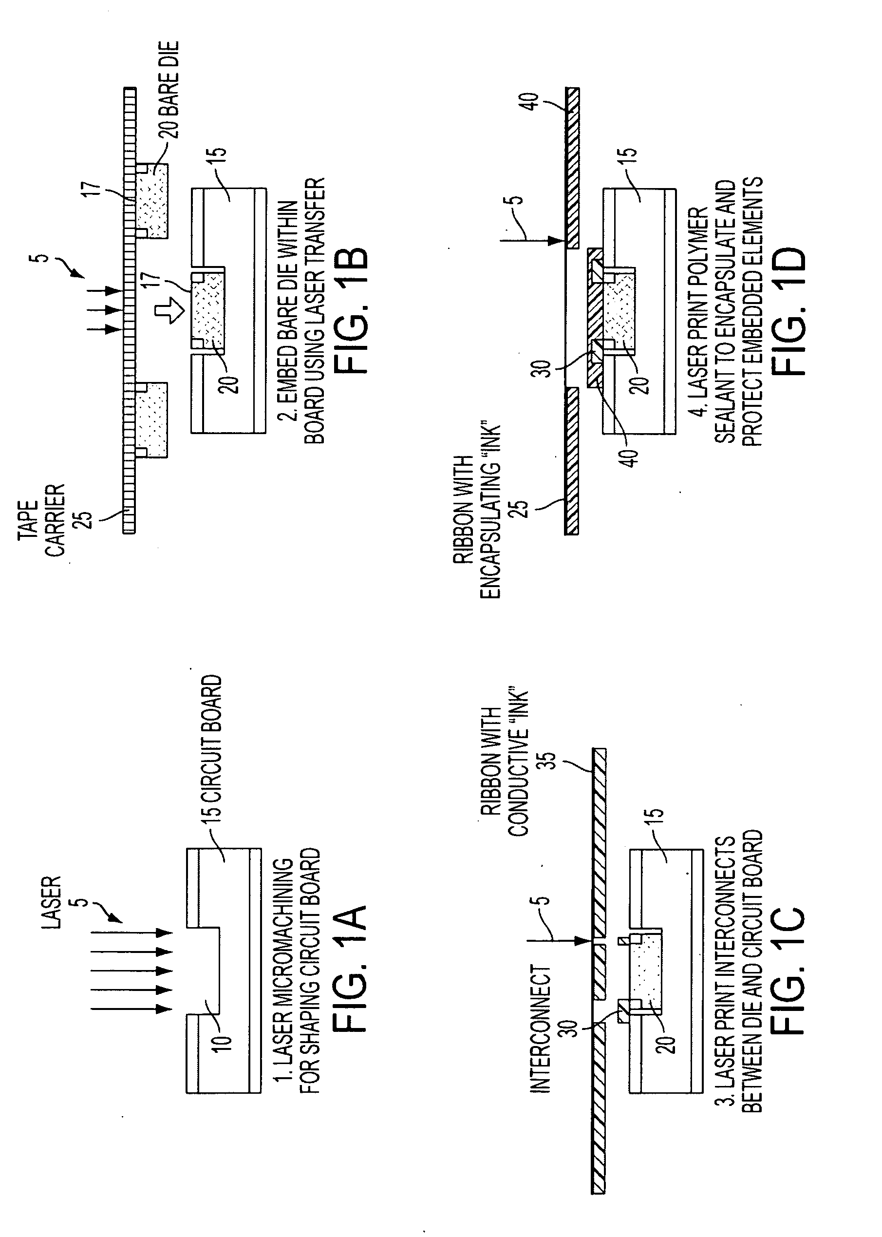
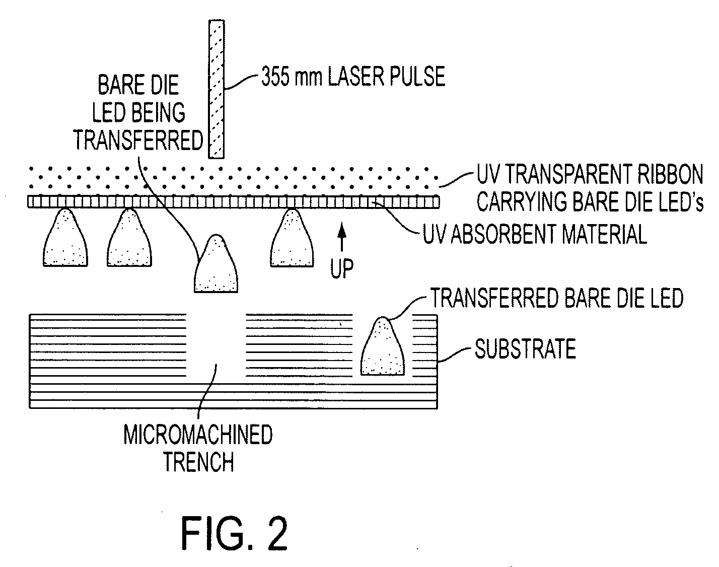
[0026]In contrast to traditional pick-and-place techniques used in populating circuit boards with the required components and devices for a given electronic circuit, the laser based technique allows for the placement and interconnection of the unpackaged components and devices inside the circuit board or any other substrate for that matter. By placing the individual components inside the substrate, i.e. embedding them, it is possible to use the substrate to protect and package the individual devices, in other words, the board becomes the package. Then the use of laser printing techniques allows the direct-write of the interconnects required by the circuit and the deposition of upper encapsulating layers (if required) thus resulting in a functional circuit embedded under the substrate surface. This laser-embedded circuit occupies a fraction of the volume of that of a circuit made with traditional manufacturing processes because the packaging required by most of its components is no l...


PUM

PropertyMeasurementUnit
thicknessaaaaaaaaaa
thickaaaaaaaaaa
thickaaaaaaaaaa

Abstract

A laser direct write method used to transfer entire single components such as semiconductor bare dies or surface mount passive and active components on a substrate or inside recess in a substrate for making embedded microelectronics is disclosed. This method laser-machine the pockets, laser-transfer the individual components inside those pockets, and then laser-print the interconnects required to “wire” the components, thus resulting in a fully assembled embedded circuit required to make a fully functional microelectronic system.

Description

CROSS-REFERENCE TO RELATED APPLICATIONS[0001]This Application is a Non-Prov of Prov (35 USC 119(e)) application 61 / 029,951 filed on Feb. 20, 2008. This Application is related to U.S. Pat. No. 6,177,151, incorporated herein in full by reference. This application is related to U.S. patent application Ser. No. 11 / 164,411, which is a divisional application of U.S. Pat. No. 6,986,199, filed on Jun. 9, 2004, allowed, which claims priority to U.S. Provisional Patent Application No. 60 / 478,471, filed on Jun. 11, 2003, both incorporated herein in full by reference. This application is related to U.S. Pat. Nos. 7,427,359, 7,001,467, and 7,014,885, all incorporated herein in full by reference.STATEMENT REGARDING FEDERALLY SPONSORED RESEARCH OR DEVELOPMENT[0002]Not applicable.REFERENCE TO A COMPACT DISK APPENDIX[0003]Not applicable.BACKGROUND OF THE INVENTION[0004]The size and weight of small, unobtrusive devices is dominated by discrete electrical components mounted to the internal circuit boa...

Claims


Application Information

Patent Timeline
Patent Type & Authority Applications(United States)
IPC IPC(8): H05K3/32
CPCH05K1/183H05K3/0032H05K3/046H05K3/321H05K2201/10106H05K2201/10477Y10T29/4913H05K2203/0338H05K2203/0528H05K2203/0537H05K2203/107Y10T29/49133Y10T29/49144H05K2201/10977H01L2224/95
Inventor PIQUE, ALBERTOMATHEWS, SCOTT A.AUYEUNG, RAYMOND C.Y.PRATAP SOOD, BHANU
Owner USA AS REPRESENTED BY THE SEC OF THE NAVY THE
Why Eureka
Try Eureka