

Novel fabrication of semiconductor quantum well heterostructure devices
a heterostructure device and semiconductor technology, applied in semiconductor lasers, instruments, lasers, etc., can solve the problems of limiting the ultimate channel width attainable in such devices, affecting their transport characteristics, and lack of control of the electron density of the channel (hole)
- Summary
- Abstract
- Description
- Claims
- Application Information
AI Technical Summary
Benefits of technology
Problems solved by technology
Method used
Image

Examples
Embodiment Construction
[0014]The following description is of the best embodiments presently contemplated for carrying out this invention. This description is made for the purpose of illustrating the general principles of this invention and is not meant to limit the inventive concepts claimed herein.
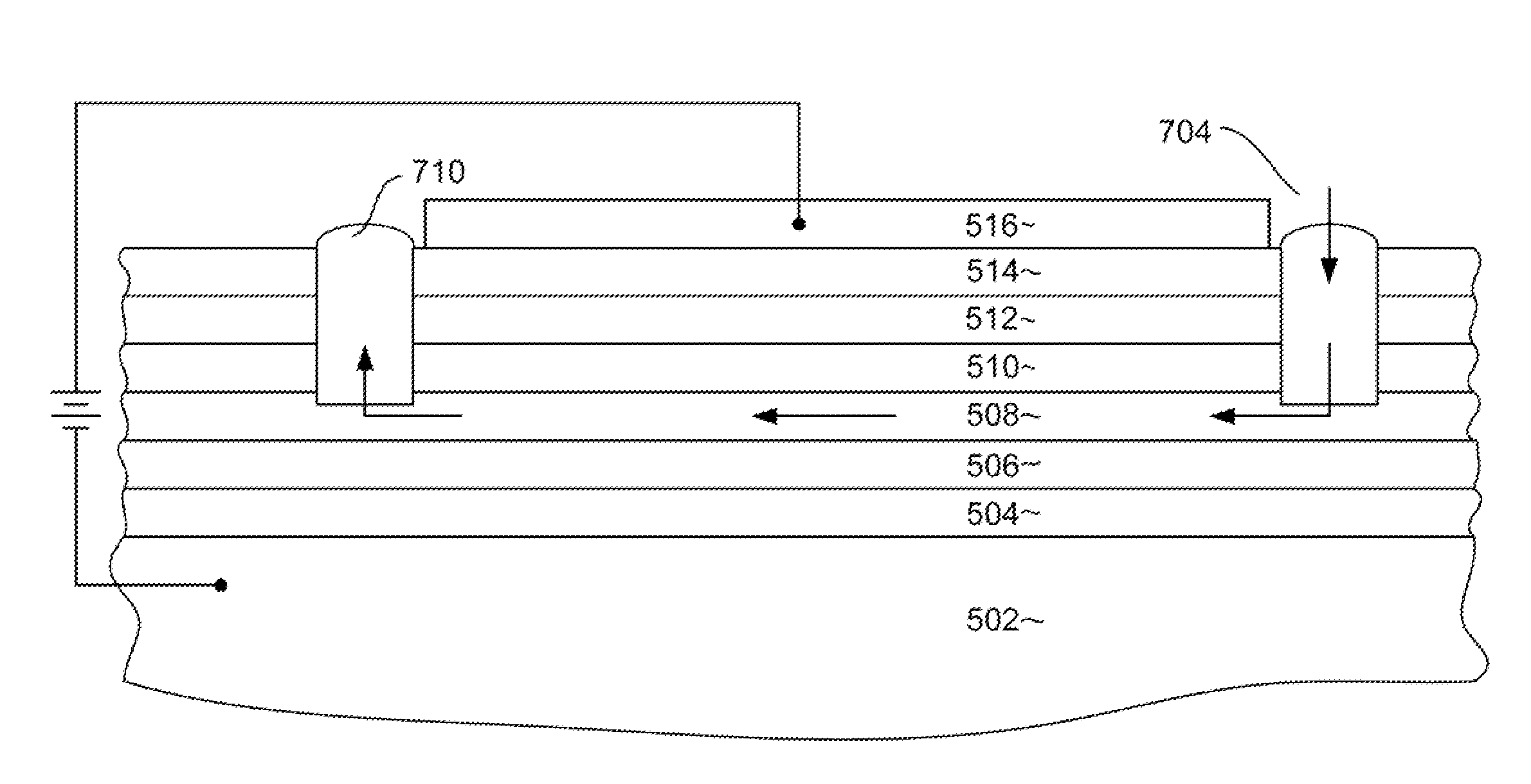
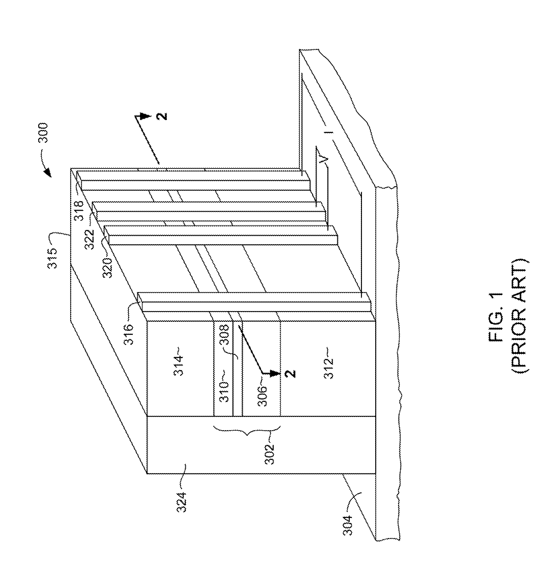
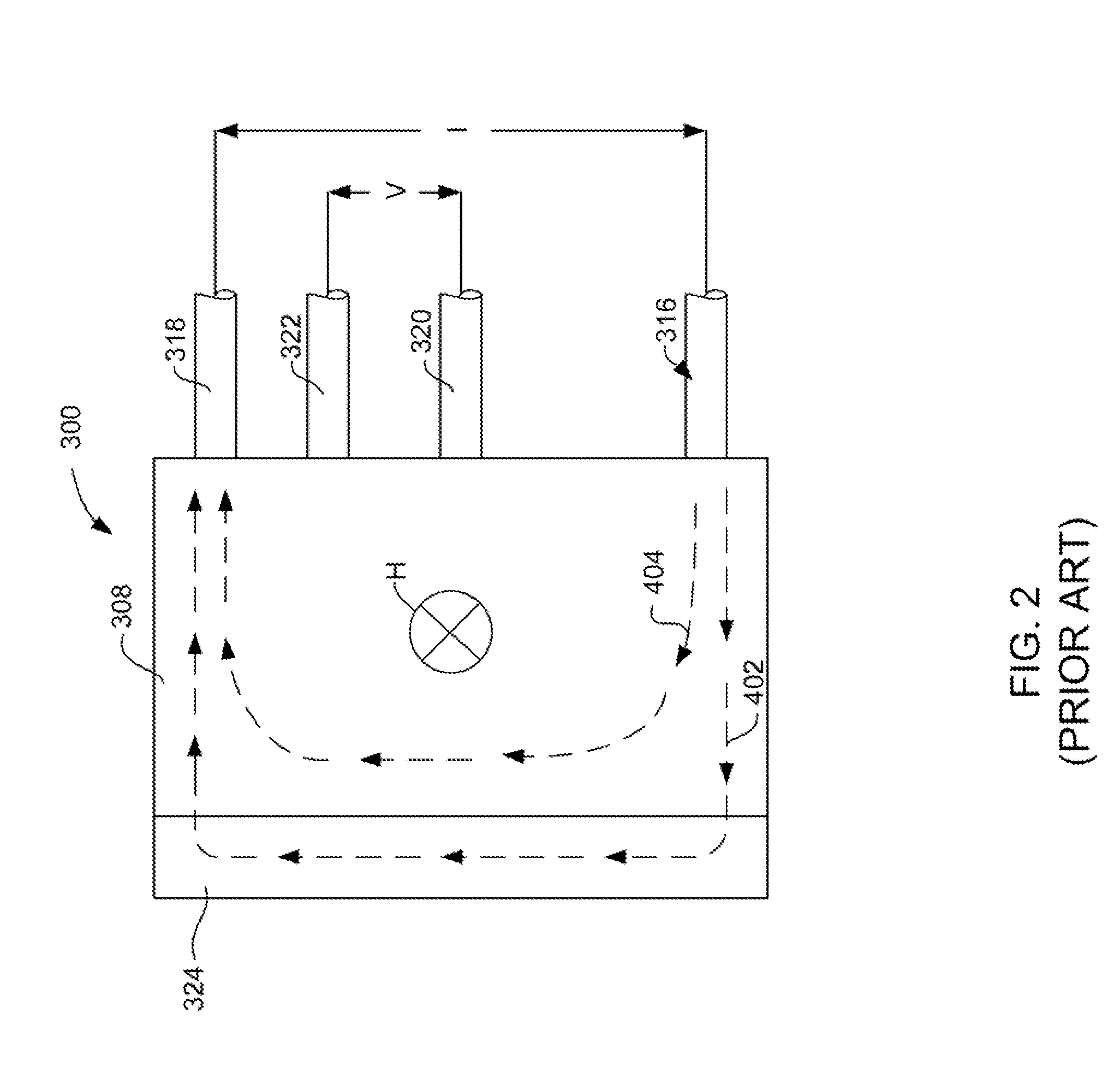
[0015]The present invention provides a mechanism for defining the active area of a device employing a quantum well structure without the need to physically pattern the semiconductor heterostructure comprising the quantum well structure itself, such as is done in mesa formation of semiconductor heterostructures. This, therefore, avoids the inherent damage caused by fabrication techniques such as reactive ion etching (RIB), ion milling, and chemical etching.
[0016]A quantum well structure can be in the form of a two dimensional electron gas (2DEG) or two dimensional hole gas. Such quantum well structures show promise for use as very small narrow and short electron (hole) channels which can be used as nano-wires in...
PUM
 Abstract
Description
Claims
Application Information