Thin-film transistor and display device

a thin film transistor and display device technology, applied in semiconductor devices, instruments, electrical apparatuses, etc., can solve the problems of insufficient switching characteristics, low on-state current, high off-state current, etc., and achieve high speed and increase the effect of field effect mobility

Inactive Publication Date: 2009-09-03
SEMICON ENERGY LAB CO LTD
View PDF7 Cites 23 Cited by
  • Summary
  • Abstract
  • Description
  • Claims
  • Application Information

AI Technical Summary

Benefits of technology

[0026]In the thin-film transistor, the field-effect mobility can be increased by increasing the donor concentration...

Problems solved by technology

The thin-film transistor in which the channel is formed in an amorphous silicon layer has a problem in that the field-effect mobility is only about 0.4 to 0.8 cm2/V·sec and the on-state current is low.
On the other hand, the thin-film transistor in which the channel is formed in a microcrystalline silicon layer has a problem in that, whereas the field-effect mobility is higher than that of the thin-film transistor using amorphous silicon, the off-state current is high, so that sufficient switching characteristics cannot be obt...

Method used


Image

  • Thin-film transistor and display device
  • Thin-film transistor and display device
  • Thin-film transistor and display device

Examples


embodiment 1

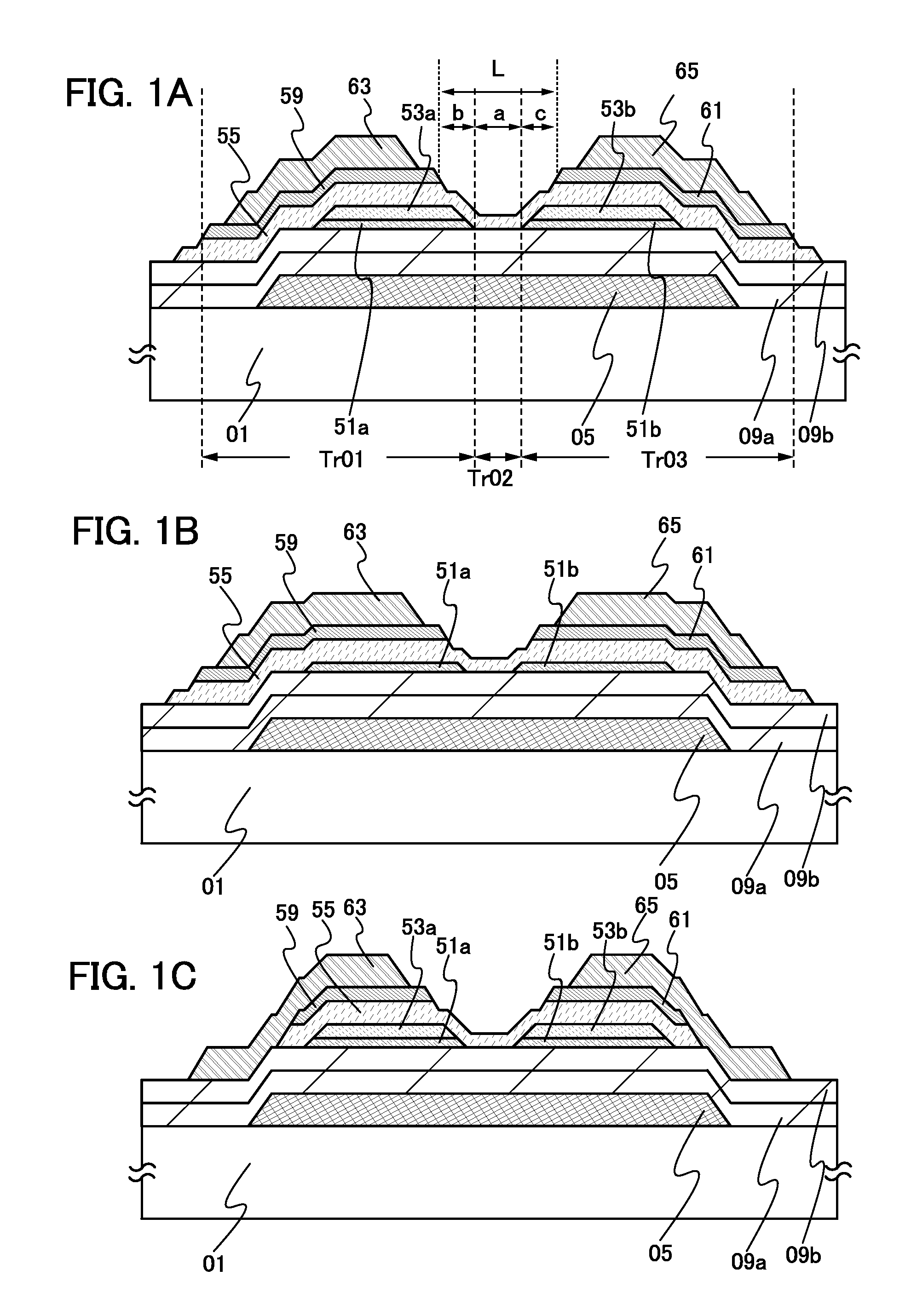
[0058]In this embodiment, structures of the thin-film transistor will be described using FIGS. 1A to 1C, in which the off-state current is lower as compared to the thin-film transistor including a microcrystalline semiconductor layer for the channel formation region and operation at higher speed can be performed and the on-state current is higher as compared to the thin-film transistor including an amorphous semiconductor layer for the channel formation region.

[0059]In a thin-film transistor shown in FIG. 1A, a gate electrode 05 is formed over a substrate 01, gate insulating layers 09a and 09b are formed over the gate electrode 05, conductive layers 51a and 51b which are provided with a space therebetween are formed over the gate insulating layer 09b, and buffer layers 53a and 53b which are provided with a space therebetween are formed over the conductive layers 51a and 51b. The buffer layers 53a and 53b are about overlapped with the conductive layers 51a and 51b. Further, an amorph...

embodiment 2

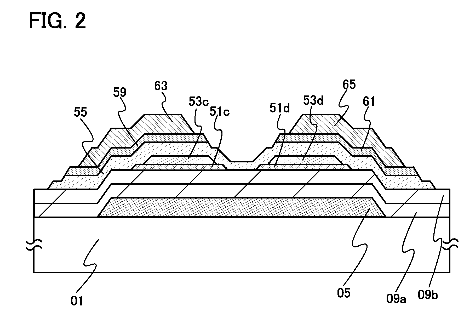
[0102]In this embodiment, other shapes of the conductive layers 51a and 51b and the buffer layers 53a and 53b will be described using FIG. 2.

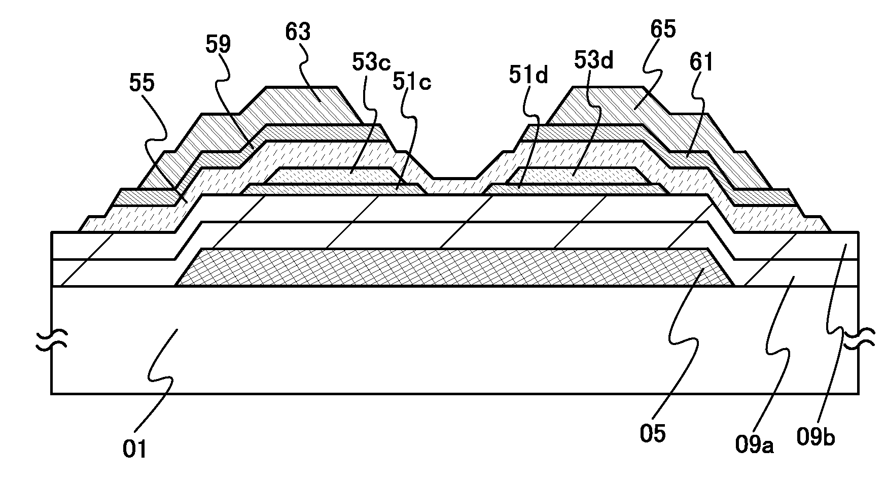
[0103]A thin-film transistor shown as a cross-sectional structure in FIG. 2 is a thin-film transistor in which a buffer layer 53c and a buffer layer 53d are formed inside of a conductive layer 51c and a conductive layer 51d provided with a space therebetween, respectively. That is, in the thin-film transistor, the buffer layers 53c and 53d each with a smaller area than each of the conductive layers 51c and 51d are formed, and the conductive layers 51c and 51d are partly exposed from the respective buffer layers 53c and 53d. With such a structure, when the conductive layers 51c and 51d are microcrystalline semiconductor layers, metal silicide layers, or metal layers, the crystallinity of the amorphous semiconductor layer 55 which is in contact with the conductive layers 51c and 51d can be improved using the microcrystalline semiconductor layers,...

embodiment 3

[0106]In this embodiment, other embodiments of the buffer layers will be described using FIGS. 3A and 3B. In this embodiment, buffer layers 52a and 52b each are formed using an insulating layer.

[0107]In a thin-film transistor shown in FIG. 3A, a gate electrode 05 is formed over a substrate 01, gate insulating layers 09a and 09b are formed over the gate electrode 05, conductive layers 51a and 51b which are provided with a space therebetween are formed over the gate insulating layer 09b, and the buffer layers 52a and 52b which are provided with a space therebetween are formed over the conductive layers 51a and 51b. The buffer layers 52a and 52b are about overlapped with the conductive layers 51a and 51b. Further, an amorphous semiconductor layer 55 which covers the side surfaces of the conductive layers 51a and 51b and the buffer layers 5S2a and 52b and the top surfaces of the buffer layers 52a and 52b is formed. A pair of impurity semiconductor layers 59 and 61 in which an impurity e...


PUM


Abstract

A thin-film transistor includes a pair of impurity semiconductor layers in which an impurity element imparting one conductivity type is added to form a source and drain regions so as to be overlapped at least partly with a gate electrode with a gate insulating layer interposed between the gate electrode and the impurity semiconductor layers; a pair of conductive layers which is overlapped over the gate insulating layers at least partly with the gate electrode and the impurity semiconductor layers, and is disposed with a space therebetween in a channel length direction; and an amorphous semiconductor layer which is in contact with the gate insulating layer and the pair of conductive layers and is extended between the pair of conductive layers.

Description

BACKGROUND OF THE INVENTION[0001]1. Field of the Invention[0002]The present invention relates to a thin-film transistor and a display device which is operated using the thin-film transistor.[0003]2. Description of the Related Art[0004]As a kind of field-effect transistor, a thin-film transistor in which a channel region is formed in a semiconductor layer formed over a substrate having an insulating surface is known. Techniques in which amorphous silicon, microcrystalline silicon, or polycrystalline silicon is used for the semiconductor layer used in the thin-film transistor have been disclosed (see Patent Documents 1 to 5). A typical application of a thin-film transistor is a liquid crystal television in which the thin-film transistor has been put to the practical use as a switching transistor for each pixel included in a display panel.[0005][Patent Document 1] Japanese Published Patent Application No. 2001-053283[0006][Patent Document 2] Japanese Published Patent Application No. He...

Claims


Application Information

Patent Timeline
IPC IPC(8): H01L33/00H01L29/786G02F1/1345G02F1/1368H01L29/417H01L29/423H01L29/49
CPCH01L27/1214H01L29/04H01L27/1288H01L29/4908H01L29/66765H01L29/458
Inventor DAIRIKI, KOJIMIYAIRI, HIDEKAZUKUROKAWA, YOSHIYUKIYAMAZAKI, SHUNPEIGODO, HIROMICHIKAWAE, DAISUKEKOBAYASHI, SATOSHI
Owner SEMICON ENERGY LAB CO LTD
Why Eureka
Try Eureka