Display device

a display device and display register technology, applied in the field of display devices, can solve the problem of naturally occurring shifts in threshold voltage, and achieve the effect of suppressing the characteristic deterioration of all transistors included in the shift register

Active Publication Date: 2009-09-10
SEMICON ENERGY LAB CO LTD
View PDF6 Cites 209 Cited by
  • Summary
  • Abstract
  • Description
  • Claims
  • Application Information

AI Technical Summary

Benefits of technology

[0073]Characteristic deterioration of all transistors included in a shift register can be suppressed. Therefore, the ma...

Problems solved by technology

However, in a case where amorphous silicon is used for a semiconductor layer of the transistor, the occurrence of a...

Method used


Image

  • Display device
  • Display device
  • Display device

Examples


embodiment mode 1

[0181]This embodiment mode describes structures and driving methods of a flip-flop, a driver circuit including the flip-flop, and a display device including the driver circuit.

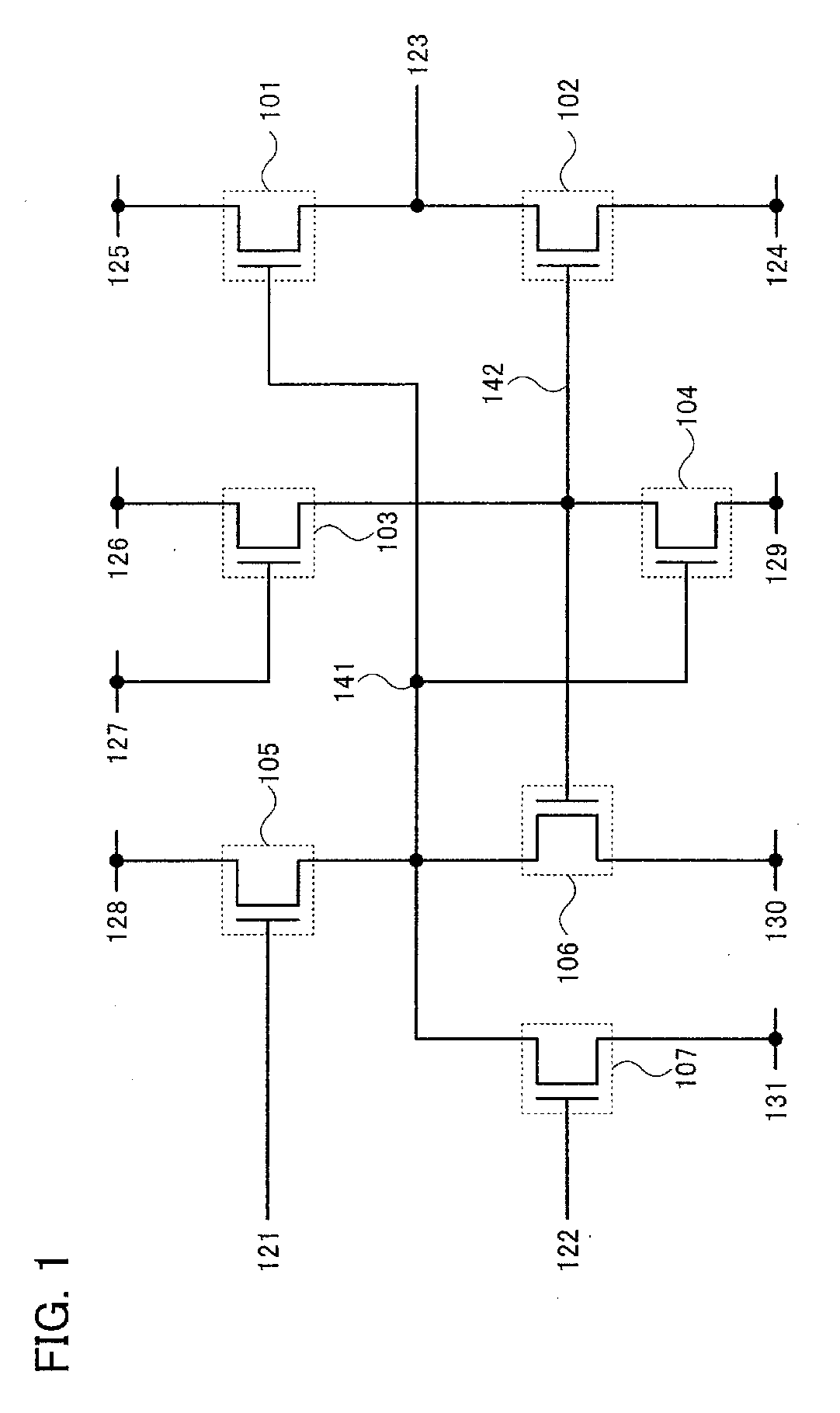
[0182]A basic structure of a flip-flop of this embodiment mode is described with reference to FIG. 1. A flip-flop shown in FIG. 1 includes a first transistor 101, a second transistor 102, a third transistor 103, a fourth transistor 104, a fifth transistor 105, a sixth transistor 106, and a seventh transistor 107. In this embodiment mode, each of the first transistor 101, the second transistor 102, the third transistor 103, the fourth transistor 104, the fifth transistor 105, the sixth transistor 106, and the seventh transistor 107 is an n-channel transistor and becomes conductive when a gate-source voltage (Vgs) exceeds a threshold voltage (Vth).

[0183]The connection relationship of the flip-flop of FIG. 1 is described. A first electrode (one of a source electrode and a drain electrode) of the first transistor ...

embodiment mode 2

[0300]This embodiment mode describes structures and driving methods of a flip-flop different from those in Embodiment Mode 1, a driver circuit including the flip-flop, and a display device including the driver circuit. Note that components in common with those in Embodiment Mode 1 are denoted by common reference numerals, and detailed description of the same portions and portions having similar functions is omitted.

[0301]A flip-flop of this embodiment mode can have a structure similar to that of the flip-flop in Embodiment Mode 1. Thus, in this embodiment mode, description of the structure of the flip-flop is omitted. Note that timing for driving the flip-flop is different from that in Embodiment Mode 1.

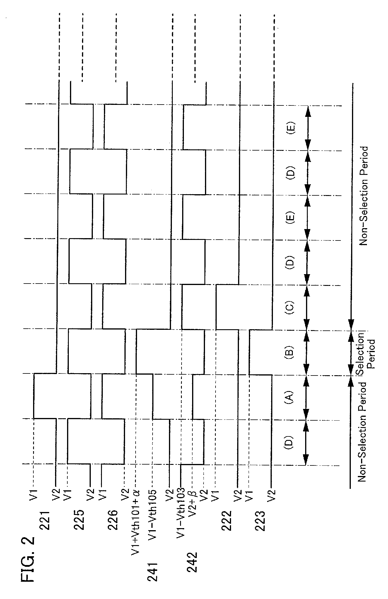
[0302]The case where driving timing of this embodiment mode is applied to the flip-flop in FIG. 1 is described. The driving timing of this embodiment mode can be freely combined with each flip-flop in FIGS. 4A to 4D, 5A to 5D, 7A to 7C, and 21A to 21C as well. Further, the driving ti...

embodiment mode 3

[0331]This embodiment mode describes structures and driving methods of a flip-flop different from those in Embodiment Modes 1 and 2, a driver circuit including the flip-flop, and a display device including the driver circuit. In the flip-flop of this embodiment mode, an output signal and a transfer signal of the flip-flop are output through different wirings by different transistors. Note that components in common with those of Embodiment Modes 1 and 2 are denoted by common reference numerals, and detailed description of the same portions and portions having similar functions is omitted.

[0332]A basic structure of the flip-flop of this embodiment mode is described with reference to FIG. 27. The flip-flop in FIG. 27 is similar to the flip-flop in FIG. 1 to which an eighth transistor 108 and a ninth transistor 109 are added.

[0333]The connection relationship of the flip-flop in FIG. 27 is described. A first electrode of the eighth transistor 108 is connected to a thirteenth wiring 133, ...


PUM


Abstract

By applying an AC pulse to a gate of a transistor which easily deteriorates, a shift in threshold voltage of the transistor is suppressed. However, in a case where amorphous silicon is used for a semiconductor layer of a transistor, the occurrence of a shift in threshold voltage naturally becomes a problem for a transistor which constitutes a part of circuit that generates an AC pulse. A shift in threshold voltage of a transistor which easily deteriorates and a shift in threshold voltage of a turned-on transistor are suppressed by signal input to a gate electrode of the transistor which easily deteriorates through the turned-on transistor. In other words, a structure for applying an AC pulse to a gate electrode of a transistor which easily deteriorates through a transistor to a gate electrode of which a high potential (VDD) is applied, is included.

Description

BACKGROUND OF THE INVENTION[0001]1. Field of the Invention[0002]The present invention relates to a display device which includes a circuit configured using a transistor. The present invention particularly relates to a display device using a light emitting element, an electro-optical element such as a liquid crystal element, or the like as a display medium and to a method for driving the display device.[0003]2. Description of the Related Art[0004]In recent years, with the increase of large-scale display devices such as liquid crystal televisions, display devices have been actively developed. In particular, a technique for forming a pixel circuit and a driver circuit including a shift register and the like (hereinafter also referred to as an internal circuit) over the same insulating substrate by using transistors formed of a non-crystalline semiconductor (hereinafter also referred to as amorphous silicon) has been actively developed because the technique greatly contributes to reduct...

Claims


Application Information

Patent Timeline
IPC IPC(8): H01L33/00G02F1/133G02F1/1345G09G3/20G09G3/36G11C19/00G11C19/28
CPCG02F1/13624G09G3/3677G09G3/3688G09G2300/0417G09G2320/043G09G2330/021H01L27/1255H01L29/42384H01L29/78696H01L27/105H01L27/12H01L27/1214H01L27/13G11C19/28H01H71/02H01H71/10H10K59/131H10K59/1213G02F1/133345G02F1/136286G02F1/1368H01L27/1222H01L27/124H01L27/1251H01L29/78678G02F1/134309G02F1/13454G02F2202/103G09G3/3266G09G2300/0426G09G2330/023H01L29/78663
Inventor UMEZAKI, ATSUSHI
Owner SEMICON ENERGY LAB CO LTD
Why Eureka
Try Eureka