Semiconductor device and method of manufacturing semiconductor device

a semiconductor and semiconductor technology, applied in the field of semiconductor devices, can solve the problems of difficult to cause selective epitaxial growth, reduce the thickness of the soi layer, and difficult to employ strain application technology, so as to improve the drive capacity, enhance the drive capacity of the mos transistor, and improve the drive capacity

Inactive Publication Date: 2009-09-10
RENESAS ELECTRONICS CORP
View PDF5 Cites 43 Cited by
  • Summary
  • Abstract
  • Description
  • Claims
  • Application Information

AI Technical Summary

Benefits of technology

[0015]According to one embodiment of the present invention, a source / drain region of a MOS transistor formed over a SOI structure which region applies to a channel region a strain for improving the drive capacity is formed by removing a buried oxide film.
[0016]According to this Embodiment, it is possible to enhance the drive capacity of a MOS transistor by forming a source / drain region for applying to a channel region a strain for improving the drive capacity and thus employing a strain application technology. The drive capacity can be enhanced further because the source / drain region is formed by removing the buried oxide film. As a result, the drive capacity of the MOS transistor can be improved even if the SOI layer becomes thinner.

Problems solved by technology

As a result of the reduction in thickness, it becomes difficult to cause selective epitaxial growth of SiGe or the like in a recessed source / drain region because the SOI layer 3 is too thin.
Although fully depleted type SOI devices have excellent characteristics such as low power consumption, high-speed operation, and small fluctuations in threshold voltage, they have a problem that a reduction in the thickness of the SOI layer makes it very difficult to employ a strain application technology.

Method used


Image

  • Semiconductor device and method of manufacturing semiconductor device
  • Semiconductor device and method of manufacturing semiconductor device
  • Semiconductor device and method of manufacturing semiconductor device

Examples


embodiment 1

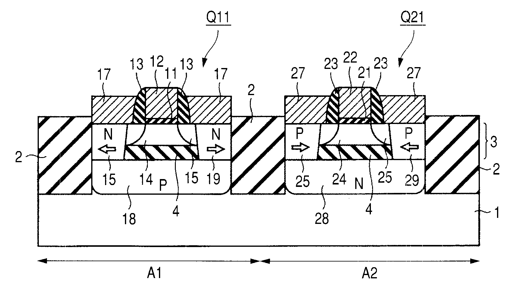
[0055]FIG. 1 is a cross-sectional view illustrating the structure of a CMOS semiconductor device of Embodiment 1 of the present invention formed over a SOI structure.

[0056]As illustrated in this drawing, in a SOI structure having a semiconductor substrate 1, a buried oxide film 4, and an element isolation insulating film 2, provided are a NMOS formation region A1 and a PMOS formation region A2 which are independent from each other, isolated by the element isolation insulating films 2 and 2 formed to penetrate through a SOI layer 3 and the buried oxide film 4 and reach a part of the semiconductor substrate 1. In these NMOS formation region A1 and PMOS formation region A2, a NMOS transistor Q11 and a PMOS transistor Q21 are formed, respectively.

[0057]First, the NMOS transistor Q11 will be described. N type source and drain regions 15 and 15 are formed selectively in the SOI layer 3 of the NMOS formation region A1. The source / drain region 15 penetrates through the buried oxide film 4 a...

embodiment 2

[0089]FIG. 15 is a cross-sectional view illustrating the structure of a CMOS semiconductor device according to Embodiment 2 of the present invention having a SOI structure.

[0090]As illustrated in this drawing, in a SOI structure having a semiconductor substrate 1, a buried oxide film 4, and an element isolation insulating film 2, a NMOS formation region A1 and a PMOS formation region A2 which are independent from each other, isolated by the element isolation insulating films 2 and 2 which penetrate through a SOI layer 3 and the buried oxide film 4, and reach a part of the semiconductor substrate 1. In these NMOS formation region A1 and PMOS formation region A2, a NMOS transistor Q12 and a PMOS transistor Q22 are formed, respectively.

[0091]First, the NMOS transistor Q12 will be described. N type source and drain regions 19 and 19 are formed selectively in the SOI layer 3 of the NMOS formation region A1. The source / drain region 19 penetrates through the buried oxide film 4 and reaches...

embodiment 3

[0115]FIG. 22 is a cross-sectional view illustrating the structure of a CMOS semiconductor device of Embodiment 3 of the present invention having a SOI structure.

[0116]As illustrated in FIG. 22, in a SOI structure comprised of a semiconductor substrate 1, a buried oxide film 4, and an element isolation insulating film 2, formed are a NMOS formation region A1 and a PMOS formation region A2 which are independent from each other, isolated by the element isolation insulating films 2 and 2 formed to penetrate through a SOI layer 3 and the buried oxide film 4 and reach a part of the semiconductor substrate 1. In these NMOS formation region A1 and PMOS formation region A2, a NMOS transistor Q12 and a PMOS transistor Q41 are formed, respectively.

[0117]Since the structure of the NMOS transistor Q12 is similar to that of the NMOS transistor Q12 of Embodiment 1 as illustrated in FIG. 15, elements having like function will be identified by like reference numerals and overlapping descriptions wi...


PUM


Abstract

Provided are a semiconductor device capable of improving the drive capacity of a MOS transistor even if the SOI layer is thinned; and a manufacturing method of the device. In a NMOS transistor formed in a NMOS formation region, a source/drain region is formed to penetrate through a buried oxide film and reach a threshold voltage controlling diffusion layer of a semiconductor substrate. In a PMOS transistor formed in a PMOS formation region, a source/drain region is formed to penetrate through a buried oxide film and reach a threshold voltage control diffusion layer of the semiconductor substrate.

Description

CROSS-REFERENCE TO RELATED APPLICATIONS[0001]The disclosure of Japanese Patent Application No. 2008-55829 filed on Mar. 6, 2008 including the specification, drawings and abstract is incorporated herein by reference in its entirety.BACKGROUND OF THE INVENTION[0002]The present invention relates to a semiconductor device having a MOS transistor formed on a SOI (Silicon on Insulator) substrate; and a manufacturing method thereof.[0003]The term “MOS” used for a metal / oxide / conductor stack structure in the past is said to be a coined acronym consisting of the initial letters of Metal-Oxide-Semiconductor. In particular, a field-effect transistor having a MOS structure (which will hereinafter be called “MOS transistor”, simply), however, uses improved materials for its gate insulating film and gate electrode from the viewpoint of recent improvement in integration degree or manufacturing process.[0004]For example, a MOS transistor uses, as a material for its gate electrode, polycrystalline s...

Claims


Application Information

Patent Timeline
Patent Type & Authority Applications(United States)
IPC IPC(8): H01L27/12H01L21/782
CPCH01L21/823807H01L21/823814H01L21/84H01L27/1203H01L29/7848H01L29/6656H01L29/66628H01L29/66636H01L29/7843H01L29/665
Inventor TSUCHIYA, RYUTA
Owner RENESAS ELECTRONICS CORP
Why Eureka
Try Eureka