
Semiconductor device for controlling supply of driving signals

a technology of magnetic field and driving signal, which is applied in the direction of pulse automatic control, dc motor rotation control, pulse technique, etc., can solve the problems of increasing power loss in output transistors, reducing the amount of power consumption in the power supply circuit, and reducing the power consumption. , to achieve the effect of reducing power consumption

Inactive Publication Date: 2009-09-10
SEIKO EPSON CORP
View PDF15 Cites 16 Cited by
  • Summary
  • Abstract
  • Description
  • Claims
  • Application Information

AI Technical Summary

Benefits of technology

[0013]Accordingly, the present invention has been accomplished focusing on solutions to the unsolved problems in the conventional technology. An advantage of the invention is to provide a semiconductor device suitable to control driving of a power supply circuit and the like at an appropriate power level according to purposes and statuses of the device.
[0014]In order to provide the advantage, according to a first aspect of the invention, there is provided a driving signal supply control semiconductor device. The driving signal supply control semiconductor device of the first aspect includes a load driving device that includes (i) a bridge circuit including a high-side first transistor and a low-side second transistor, the transistors being electrically connected to a load as an object to be driven and being turned on or off to energize or de-energize the load; (ii) a first driving circuit driving the first transistor; (iii) a second driving circuit driving the second transistor; (iv) a first power supply circuit supplying driving power to the first driving circuit; (v) a second power supply circuit supplying driving power to the second driving circuit; (vi) a supply content setting unit setting a supply content of each of driving signals regarding low-power driving of the load driving device, according to a standby status of the load; and (vii) a driving signal supply control unit controlling supply of the driving signals to the first and the second power supply circuits, the driving signal supply control unit controlling independently contents of the driving signals supplied to each of the first and the second power supply circuits such that the load driving device is driven with lower power consumption than in a normal driving status of the load driving device, based on the supply content set by the supply content setting unit.
[0015]In the semiconductor device of the first aspect, according to the
[0016]standby status of the load, the supply content setting unit sets a predetermined supply content. Then, based on the set supply content, the driving signal supply control unit supplies the driving signals containing the supply content that allows the load driving device to be driven with lower power consumption than in the normal driving status, independently to each of the first and the second power supply circuits.
[0017]For example, while allowing the first power supply circuit to be driven
[0018]in a normal driving status, an amount of a bias current signal (the driving signal) supplied to the second power supply circuit is reduced to less than in the normal driving status. Thereby, as compared to the conventional technology, the load driving device in the first aspect can return from the low-power driving status to the normal driving status in a shorter time, as well as the individual circuits can be driven with low power consumption.

Problems solved by technology

Since power consumption of a driving circuit section increases upon operation, power loss in the output transistors also increases.
Returning to normal operation takes time, thereby delaying response time until the load can be driven upon restarting.
Thus, the amount of power consumption in the power supply circuit cannot be reduced.
first and the second power supply circuits to allow the load driving device to be driven with low power consumption results in low-power driving of the power supply circuits.
In this case, the amount of power consumption is increased than in the setting of the first supply content.
Furthermore, controlling the driving signals supplied to the first and the second bias voltage supply circuits so as to drive the load driving device with low power ultimately results in low-power driving of the first and the second power supply circuits.

Method used


Image

  • Semiconductor device for controlling supply of driving signals
  • Semiconductor device for controlling supply of driving signals
  • Semiconductor device for controlling supply of driving signals

Examples


Embodiment Construction

[0082]Embodiments of the invention will be described with reference to the drawings. FIGS. 1 to 9 are diagrams showing a driving signal supply control semiconductor device according to an embodiment of the invention.

[0083]In the present embodiment, a motor driving device is applied to the driving signal supply control semiconductor device of the embodiment. The motor driving device includes an H-bridge circuit that controls driving of the motor.

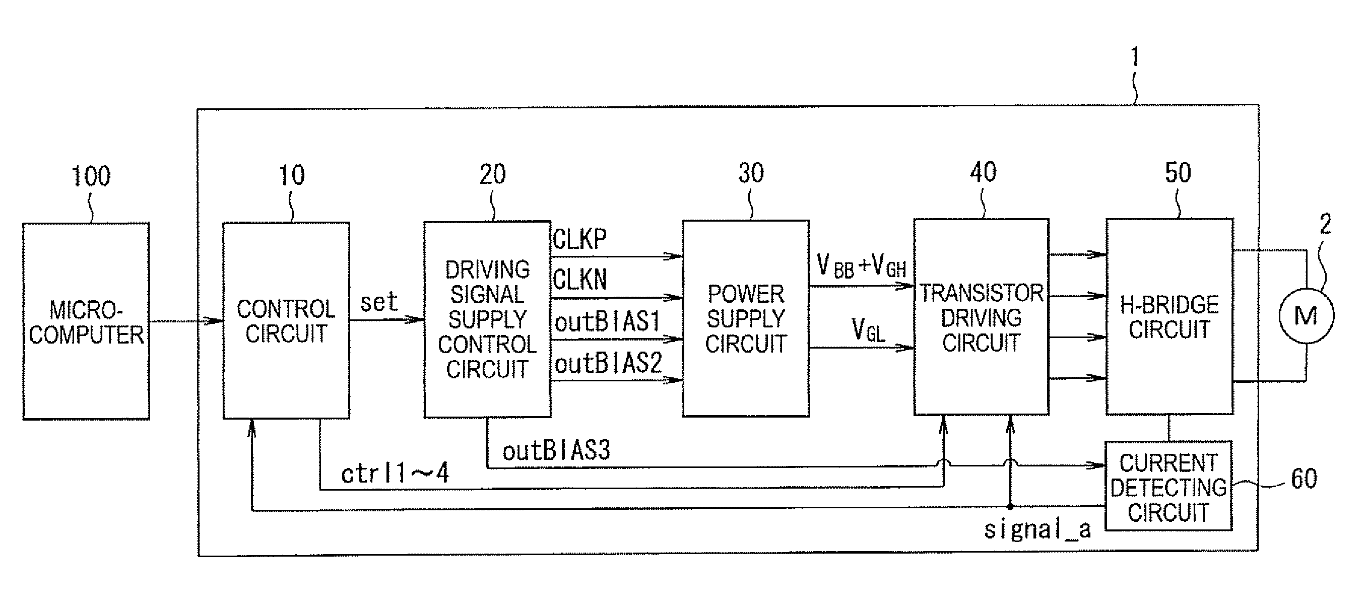
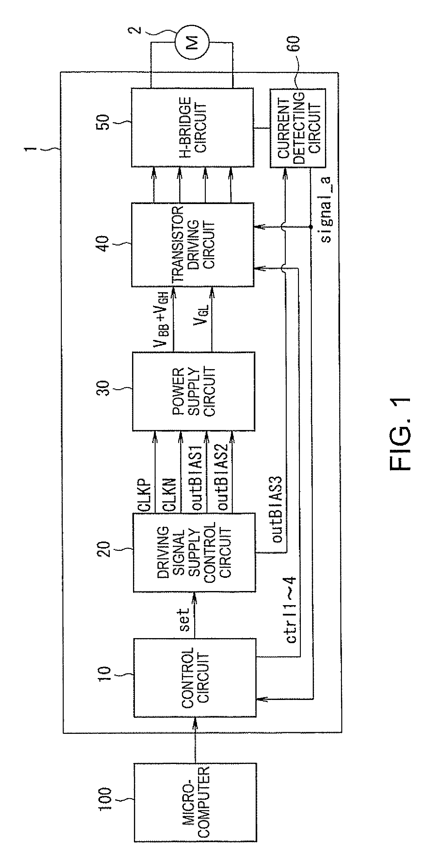
[0084]First, a structure of a motor driving device 1 according to the embodiment will be described with reference to FIG. 1. FIG. 1 is a block diagram showing a structure of the motor driving device 1.

[0085]As shown in FIG. 1, the motor driving device 1 includes a control circuit 10, a driving signal supply control circuit 20, a power supply circuit 30, a transistor driving circuit 40, an H-bridge circuit 50, and a current detecting circuit 60.

[0086]The control circuit 10 includes a serial interface circuit to be connected to an external micr...


PUM


Abstract

A driving signal supply control semiconductor device includes a load driving device that includes: (i) a bridge circuit including a high-side first transistor and a low-side second transistor, the transistors being electrically connected to a load as an object to be driven and being turned on or off to energize or de-energize the load; (ii) a first driving circuit driving the first transistor; (iii) a second driving circuit driving the second transistor; (iv) a first power supply circuit supplying driving power to the first driving circuit; (v) a second power supply circuit supplying driving power to the second driving circuit; (vi) a supply content setting unit setting a supply content of each of driving signals regarding low-power driving of the load driving device, according to a standby status of the load; and (vii) a driving signal supply control unit controlling supply of the driving signals to the first and the second power supply circuits. Based on the supply content set by the supply content setting unit, the driving signal supply control unit controls independently contents of the driving signals supplied to each of the first and the second power supply circuits such that the load driving device is driven with lower power consumption than in a normal driving status of the load driving device.

Description

BACKGROUND[0001]1. Technical Field[0002]The present invention relates to a driving signal supply control[0003]semiconductor device suitable to reduce the amount of power consumption of a constant voltage power supply circuit used when driving a driving device that includes a bridge circuit driving a load such as a motor.[0004]2. Related Art[0005]Conventionally, as circuits driving a load such as a motor, there are[0006]known as a half-bridge circuit, a full-bridge circuit, and the like. Those circuits include a high-potential-side (high-side) transistor and a low-potential-side (low-side) transistor. The high-side and the low-side transistors are independently controlled to be driven so as to be turned on or off, thereby energizing or de-energizing the load.[0007]Additionally, a load requiring a relatively high power for high-speed switching operation uses metal-oxide-semiconductor field-effect transistors (MOSFETs) designed for high-current applications, as transistors included in ...

Claims


Application Information

Patent Timeline
IPC IPC(8): H03L5/02
CPCH02M7/538H02M2001/0032Y02B70/16H03K17/693H02P7/0044H02P7/04Y02B70/10H02M1/0032
Inventor YONEYAMA, TSUYOSHIYAMADA, ATSUSHI
Owner SEIKO EPSON CORP
Learn More