Method for the preparation of nanostructures and nanowires

a nanostructure and nanowire technology, applied in the field of nanostructures and nanowires, can solve the problems of not being suitable for nanowire production, not being cost-effective in obtaining nanoscale wires within the aperture, and the process is rather complicated to operate, etc., and is not suitable for using the whole structur

Inactive Publication Date: 2009-09-17
ISTANBUL TEKNIK UNIVSI
View PDF3 Cites 10 Cited by
  • Summary
  • Abstract
  • Description
  • Claims
  • Application Information

AI Technical Summary

Benefits of technology

[0013]A further object of the present invention is to provide a method for the fabrication of the nanowires and nanopatterned functional surfaces, wherein a unique etchant solution etches the inner walls and bo

Problems solved by technology

The process provides an effective way to obtain a nanostructure for use as a filter, however the process is rather complicated to operate and is not cost effective in terms of obtaining nano scale wires within the apertures of the nanoholes.
However, it is well known in the art that such lithographic applications damage the nanostructure in an undesired way

Method used


Image

  • Method for the preparation of nanostructures and nanowires
  • Method for the preparation of nanostructures and nanowires
  • Method for the preparation of nanostructures and nanowires

Examples


example 1

Preparation of the Oxidized Nanostructure Suitable for Metal Electro-Deposition

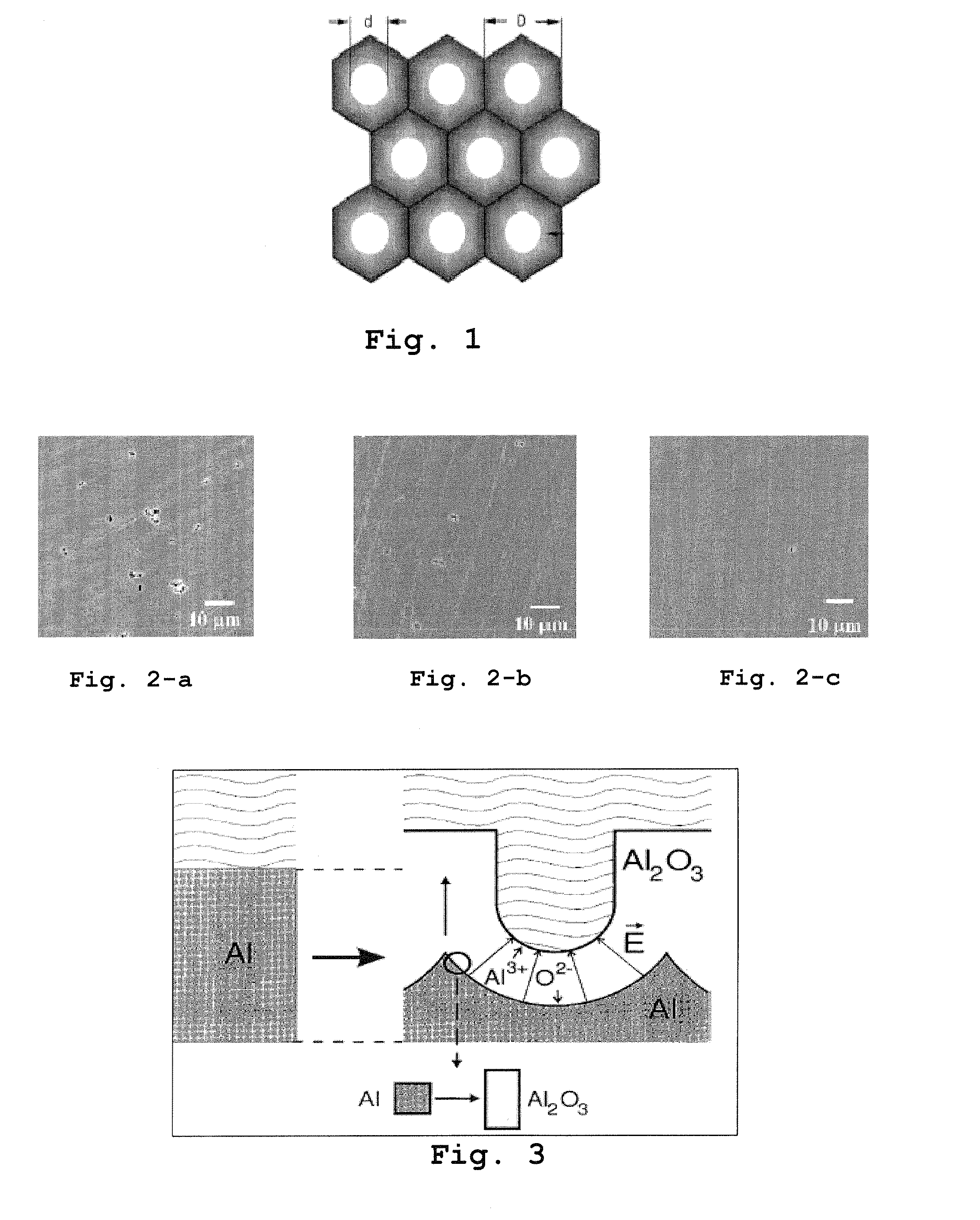
[0051]Aluminum sheets having the size of 7×4 cm and thickness of 0.5 mm were used as the substrates during the experimental procedure. The substrates used for this purpose were supplied from Assan Alüminyum San. A.S.-Istanbul Turkiye, as 1050 series aluminum sheets which have the following specific composition;

AlFeSiCuMgMnZnVTiOthers99.50.40.250.050.050.050.050.050.030.03minmaxmaxmaxmaxmaxmaxmaxmaxmax

[0052]Aluminum sheets are subjected to the cleaning steps prior to the anodization procedure. Sheets are immersed into a 40 g / L NaOH solution at 55° C. for 2 minutes and then washed with purified water. Samples are polished by way of immersing the same into a 15% (by volume) HNO3 solution for 30 seconds and washed again with distilled water. Anodization experiments were conducted twice with a 72V-12 A DC source in a double walled cooling bath wherein the temperature was controlled with a thermostat having ±0....

example 2

Metal Electro-Deposition and Manufacturing of Nanowires

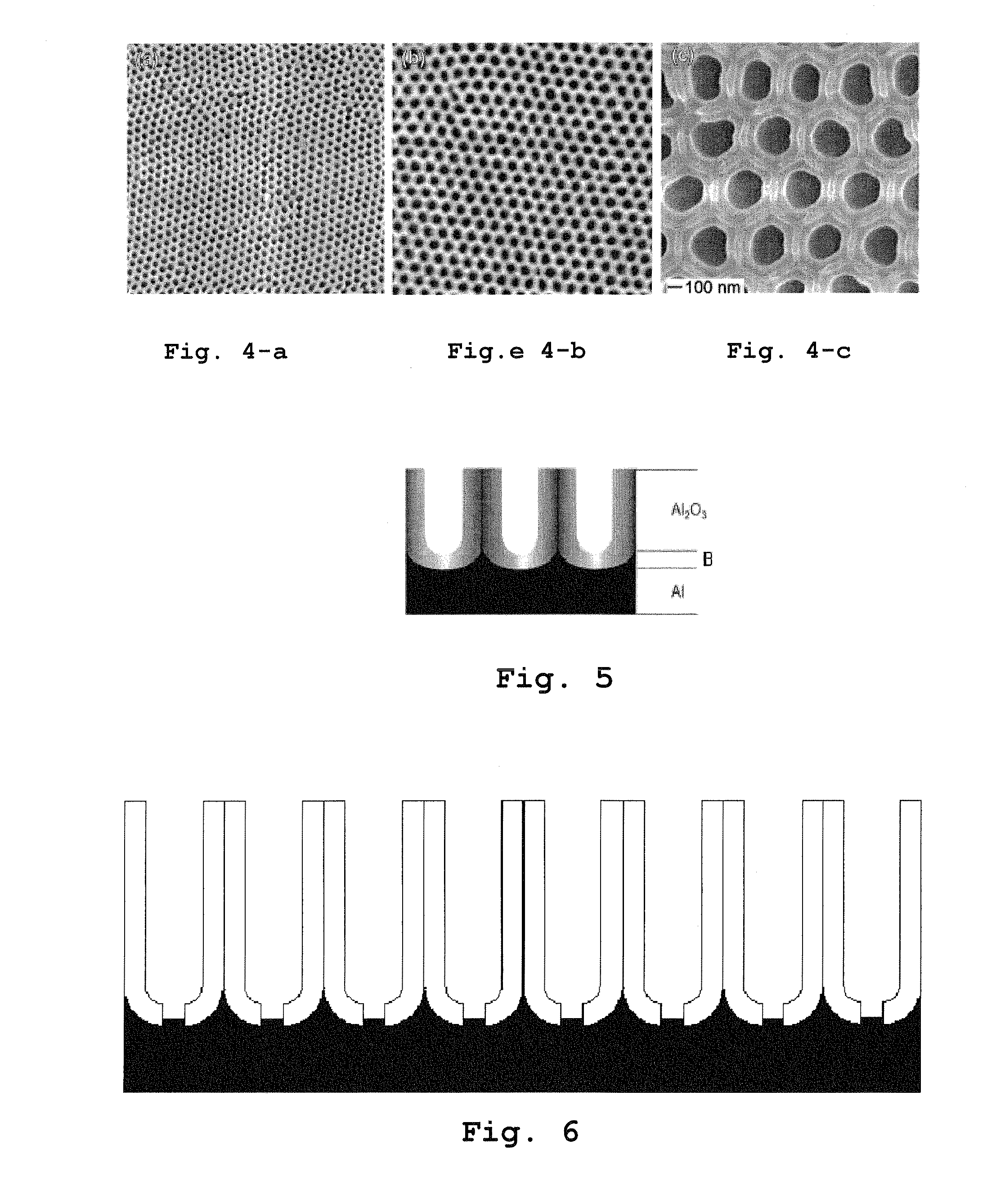
[0056]The porous nanostructure which was made electronically conductive for 60 seconds in the previous example was subjected to an electrolytic metal deposition step wherein said structure was utilized as the cathode and Ni was utilized as the anode electrode. Electrolytic solution bath was containing 300 g / L NiSO4 and 45 g / L H3BO3 and said solution was heated to 50° C. before starting the electrolytic process. Two pieces of nanostructure sheets were used in the process in order to observe the amount of metal deposition depending on the current density. One of the pieces was subjected to 2 A / dm3 and the other one was subjected to 0.2 A / dm2 current densities for this purpose. Pieces were washed right after the electrolytic process and analyzed with Scanning Electron Microscope. Results are shown in FIGS. 10-a and 10-b wherein the nanowires formed in 2 A / dm2 current density and the nanowires formed in 0.2 A / dm2 current density are...


PUM

PropertyMeasurementUnit
Fractionaaaaaaaaaa
Fractionaaaaaaaaaa
Fractionaaaaaaaaaa

Abstract

A process for producing porous nanostructures suitable for the manufacture of nanowires and processes for manufacturing of the nanowires by using said nanostructure are disclosed. The process for obtaining the nanostructure of the invention comprises the steps of cleaning and polishing the surface of an aluminum metal substrate, forming a porous oxide layer bearing nanoholes on said aluminum substrate, immersing the porous structure into a basic zincate solution for etching the bottoms and walls of the nanoholes and depositing a thin and substantially pure Zn film extending from the bottom of the nanoholes through the aluminum substrate. Nanowires can be fabricated by the step of utilizing so obtained etched nanostructure as an electrode and subjecting the same to a metal electro-deposition operation.

Description

TECHNICAL FIELD OF THE INVENTION[0001]The present invention relates to an improved method for producing nanostructures bearing regular arrays of pores, and method of electrochemical metal or alloy deposition within said pores in order to form nano scale patterns and nanowires. The present invention is characterized by the principle of etching pore walls and bottoms by using a unique solution and making the same electro-conductive by forming a Zn film extending from inner walls of the pores through the substrate layer. The solution of the invention enables to provide the metal deposition with simplified and efficient electrolytic plating processes.BACKGROUND AND SUMMARY OF THE INVENTION[0002]Nanostructures, which consist of a porous alumina oxide film on a substantially pure substrate are conventionally produced according to a number of well known methods such as electrochemical anodization of aluminum or various lithographic techniques. Also a number of methods have been developed i...

Claims


Application Information

Patent Timeline
IPC IPC(8): C25D5/00C25D11/02
CPCB82Y30/00C25D11/20C25D1/04C23F1/36
Inventor URGEN, MUSTAFAYESIL, YASIN
Owner ISTANBUL TEKNIK UNIVSI
Why Eureka
Try Eureka