Device having active region with lower electron concentration

a technology of active region and electron concentration, which is applied in the direction of semiconductor/solid-state device details, radio-controlled devices, nuclear engineering, etc., can solve the problems of thz sources that are bulky, can only operate at cryogenic temperatures, and can only operate at high temperature. , the effect of reducing the efficiency of thz sources

Active Publication Date: 2009-09-17
SENSOR ELECTRONICS TECH
View PDF59 Cites 18 Cited by
  • Summary
  • Abstract
  • Description
  • Claims
  • Application Information

AI Technical Summary

Benefits of technology

[0006]Aspects of the invention provide a device comprising a two-dimensional electron gas that includes an active region located in a portion of the electron gas. The active region comprises an electron concentration less than an electron concentration of a set of non-active regions of the electron gas. The device includes a controlling terminal located on a first side of the active region. The device can comprise, for example, a field effect transistor (FET) in which the gate is located and used to control the carrier injection into the active region and define the boundary condition for the electric field distribution within the active region. The device can be used to generate, amplify, filter, and / or detect electromagnetic radiation of radio frequency (RF) and / or terahertz (THz) frequencies.

Problems solved by technology

However, to date, there is lack of fast solid state devices operating at these frequencies that can be used to build relatively cheap, fast and compact spectroscopic systems.
As a result, most THz sources are bulky, fairly effective, and can only operate at cryogenic temperatures.
Due to specific material related issues of GaAs, these devices have frequency limitations in the THz frequency range making them practically useless even at sub-terahertz frequencies without frequency multipliers, and extremely inefficient at frequencies above 100 gigahertz (GHz).
Also, Gunn effect devices with large cross-sections have significant coherency problems and skin effect related issues.

Method used


Image

  • Device having active region with lower electron concentration
  • Device having active region with lower electron concentration
  • Device having active region with lower electron concentration

Examples


Embodiment Construction

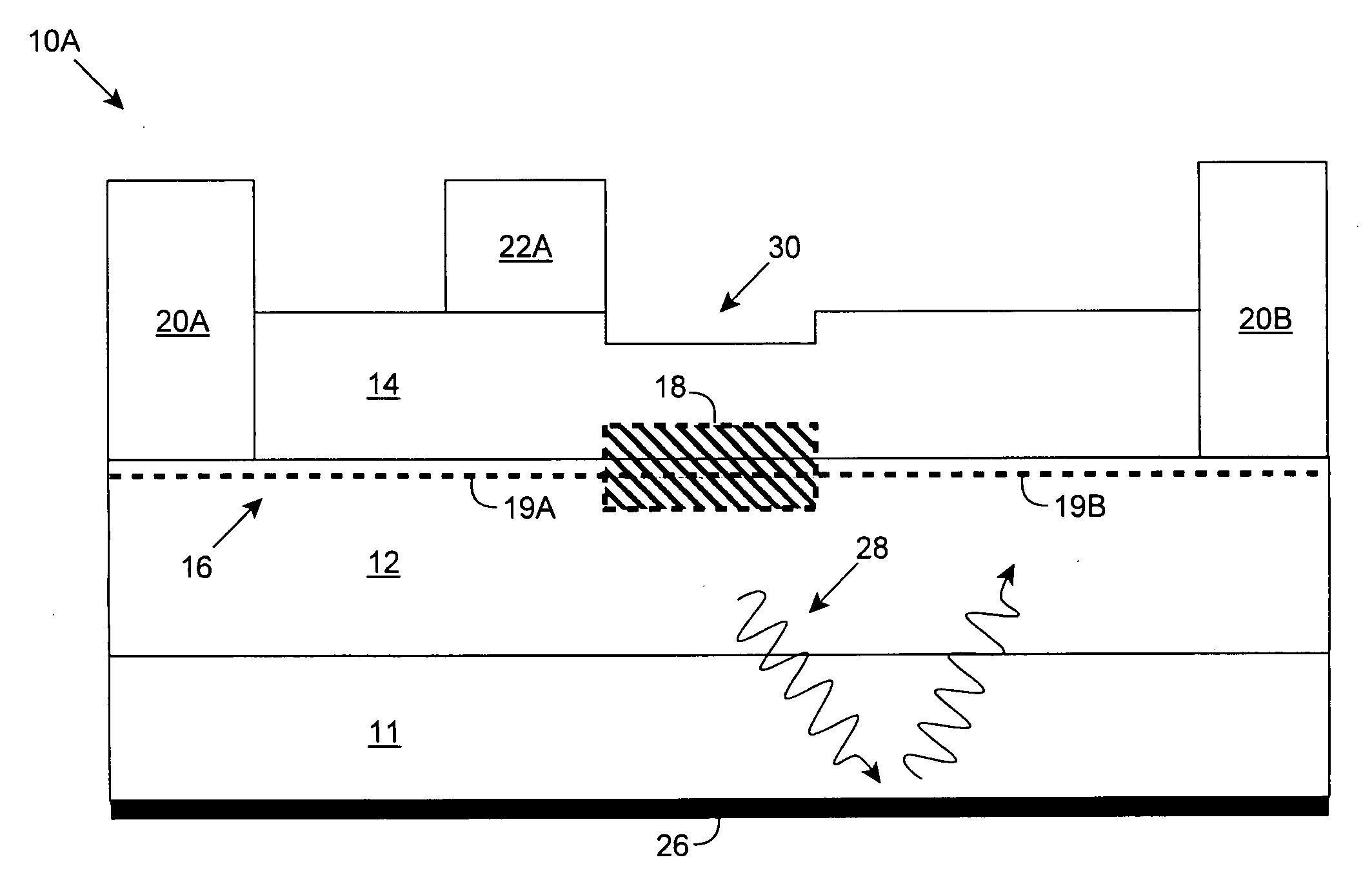
[0019]As indicated above, aspects of the invention provide a device comprising a two-dimensional electron gas that includes an active region located in a portion of the electron gas. The active region comprises an electron concentration less than an electron concentration of a set of non-active regions of the electron gas. The device includes a controlling terminal located on a first side of the active region. The device can comprise, for example, a field effect transistor (FET) in which the gate is located and used to control the carrier injection into the active region and define the boundary condition for the electric field distribution within the active region. The device can be used to generate, amplify, filter, and / or detect electromagnetic radiation of radio frequency (RF) and / or terahertz (THz) frequencies. As used herein, unless otherwise noted, the term “set” means one or more (i.e., at least one) and the phrase “any solution” means any now known or later developed solutio...


PUM


Abstract

A device comprising a two-dimensional electron gas that includes an active region located in a portion of the electron gas is disclosed. The active region comprises an electron concentration less than an electron concentration of a set of non-active regions of the electron gas. The device includes a controlling terminal located on a first side of the active region. The device can comprise, for example, a field effect transistor (FET) in which the gate is located and used to control the carrier injection into the active region and define the boundary condition for the electric field distribution within the active region. The device can be used to generate, amplify, filter, and/or detect electromagnetic radiation of radio frequency (RF) and/or terahertz (THz) frequencies.

Description

REFERENCE TO PRIOR APPLICATION[0001]The current application claims the benefit of co-pending U.S. Provisional Application No. 61 / 069,101, titled “Two-dimensional semiconductor oscillator,” which was filed on 12 Mar. 2008, and which is hereby incorporated by reference.TECHNICAL FIELD[0002]The disclosure relates generally to high power, high frequency solid state devices, and more particularly, to tens to thousands micrometer radio-frequency (RF) and terahertz frequency oscillators, amplifiers, and detectors capable of operating at room temperature.BACKGROUND ART[0003]Devices that function as sources, amplifiers, and detectors of terahertz (THz) and millimeter wave radiation are of great interest due to potential applications for systems that utilize such devices. For example, a spectroscopic system operating at such ranges of radiation can detect complex chemical and biological compounds, live objects, and other features. Current applications of THz spectroscopy also include such imp...

Claims


Application Information

Patent Timeline
Patent Type & Authority Applications(United States)
IPC IPC(8): G21G4/00H01L29/66H01L21/335
CPCH01L29/0657H01L29/2003H01L29/7831H01L29/518H01L29/7787H01L29/207
Inventor KOUDYMOV, ALEXEISHUR, MICHAELGASKA, REMIGIJUS
Owner SENSOR ELECTRONICS TECH
Why Eureka
Try Eureka