Duty cycle correction circuit and semiconductor integrated circuit apparatus including the same
- Summary
- Abstract
- Description
- Claims
- Application Information
AI Technical Summary
Benefits of technology
Problems solved by technology
Method used
Image
Examples
Embodiment Construction
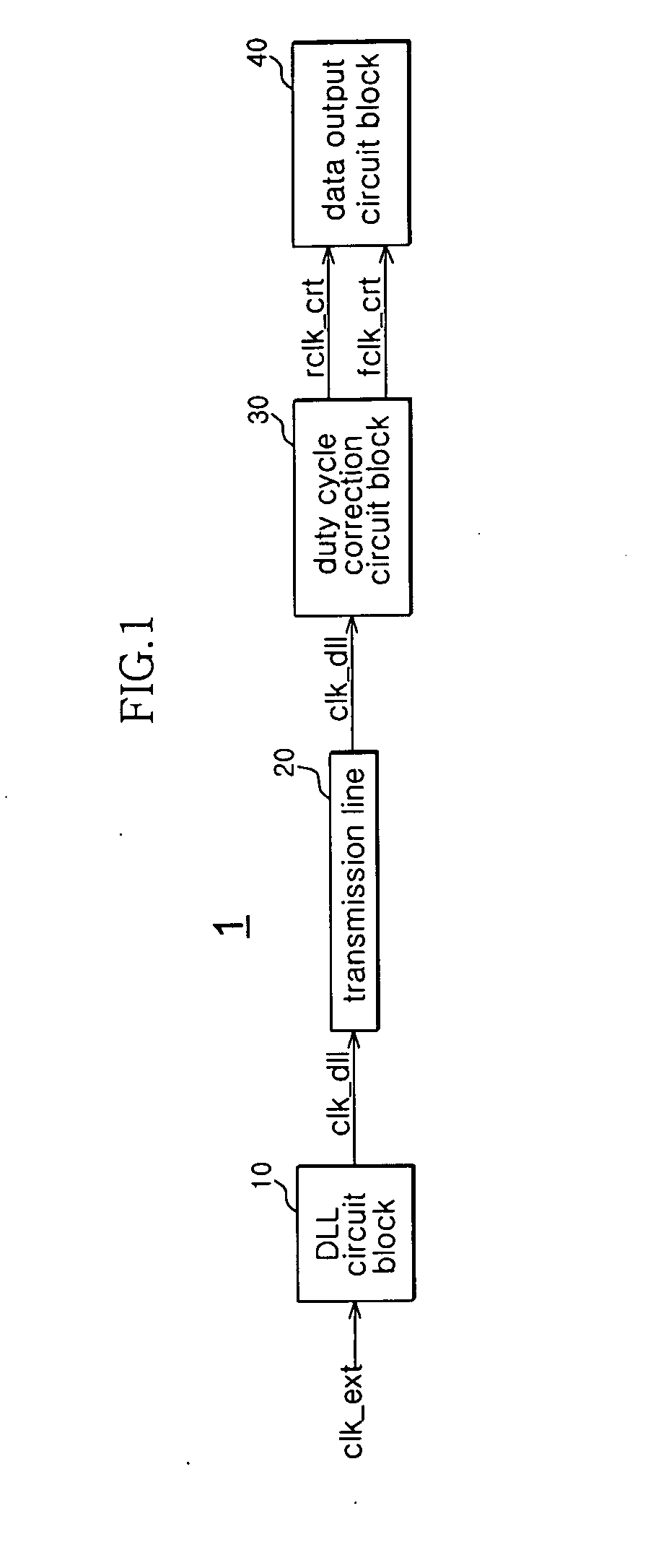
[0017]FIG. 1 is a schematic block diagram of an exemplary semiconductor integrated circuit apparatus according to one embodiment. In FIG. 1, a semiconductor integrated circuit apparatus 1 can include a DLL circuit block 10, a transmission line 20, a duty cycle correction circuit block 30, and a data output circuit block 40.
[0018]The DLL circuit block 10 can be configured to generate a DLL clock signal ‘clk_dll’ having a phase faster than a phase of an external clock signal ‘clk_ext’ by a predetermined time. Here, the DLL clock signal ‘clk_dll’ can have a single signal configuration instead of a clock signal pair.
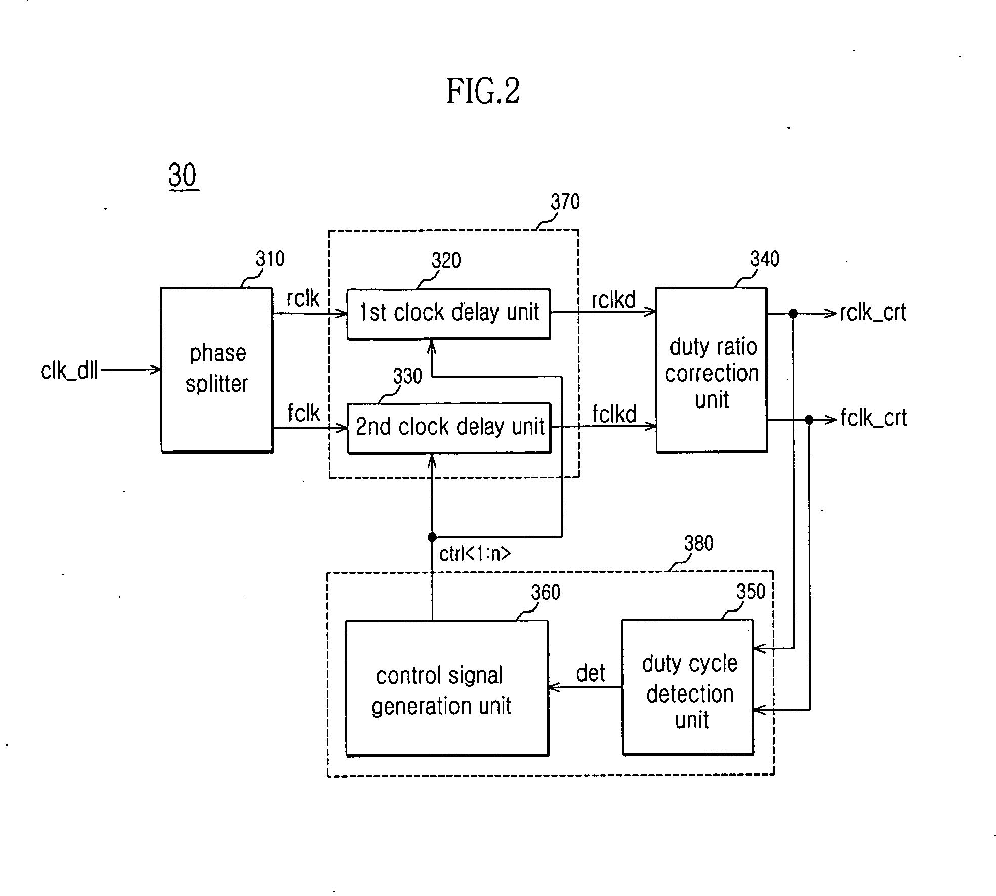
[0019]The transmission line 20 can be configured to transmit the DLL clock signal ‘clk_dll’ to the duty cycle correction circuit block 30 to correct the duty cycle of the DLL clock signal ‘clk_dll’ and then generate a correction rising clock signal ‘rclk_crt’ and a correction falling clock signal ‘fclk_crt’. The duty cycle correction circuit block 30 can be configured to con...
PUM
 Abstract
Description
Claims
Application Information


