Optical receiver for regeneration of optical signal
a technology of optical signal and optical receiver, which is applied in the field of optical receiver, can solve the problems of data error due to optical noise becoming a bottleneck for dwdm transmission, significant increase in interference between wavelength channels, and serious deterioration of optical signal to noise ratio (osnr)
- Summary
- Abstract
- Description
- Claims
- Application Information
AI Technical Summary
Benefits of technology
Problems solved by technology
Method used
Image
Examples
first embodiment
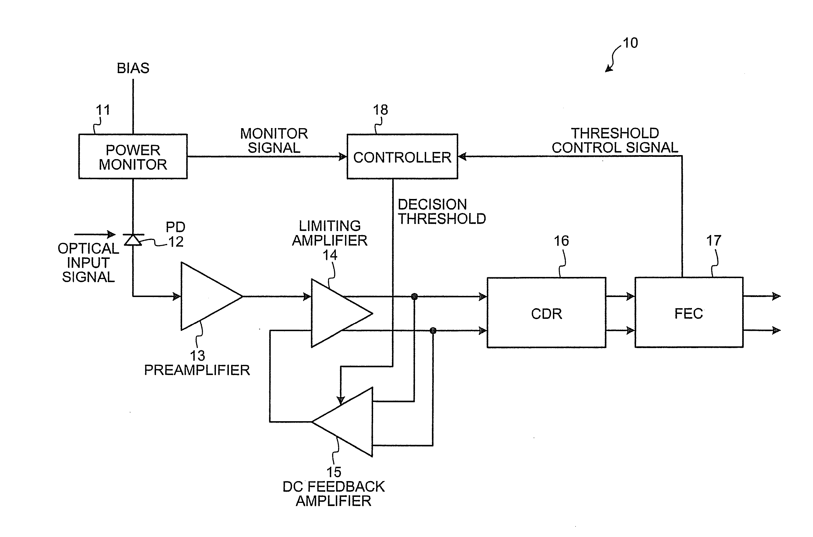
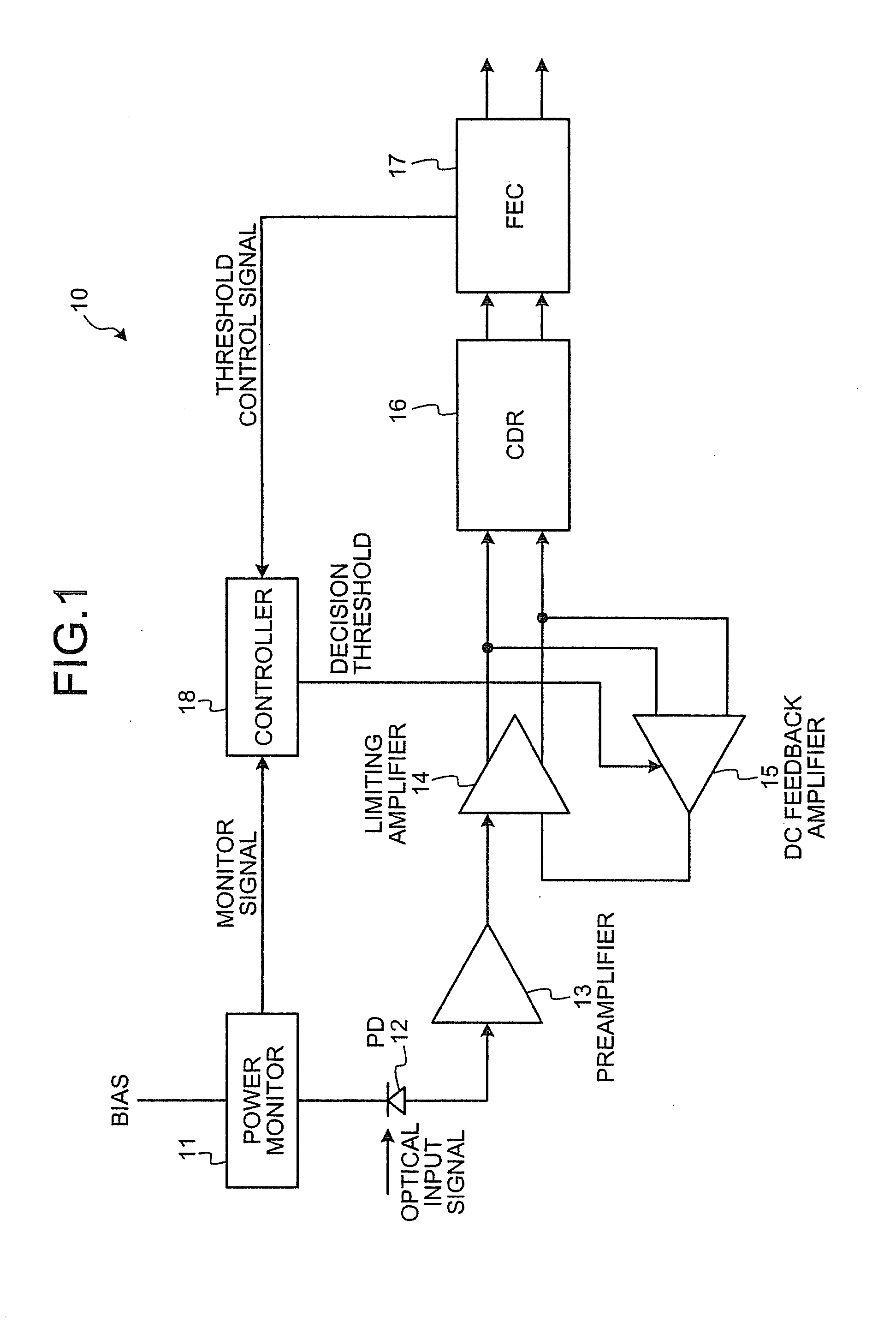
[0031]FIG. 1 is a block diagram of an optical receiver according to the present invention. An optical receiver 10 includes a power monitor 11, a photodiode (PD) 12, a preamplifier 13, a limiting amplifier 14, a direct current (DC) feedback amplifier 15, a clock / data recovery (CDR) 16, a forward error correction (FEC) unit 17, and a controller 18.
[0032]The PD 12 converts an optical input signal into an electrical signal. The preamplifier 13 and the limiting amplifier 14 amplify the electrical signal. An output signal from the preamplifier 13 is input to one of the input terminals of the limiting amplifier 14. The DC feedback amplifier 15 feedbacks an output signal from the limiting amplifier 14 back to the other input terminal of the limiting amplifier 14. Thus, the DC feedback amplifier 15 controls the DC level of the positive signal and the negative signal output from the limiting amplifier 14. The CDR 16 regenerates and retimes the output signal from the limiting amplifier 14.
[003...
fourth embodiment
[0044]FIG. 10 is a block diagram of an optical receiver according to the present invention. An optical receiver 40 shown in FIG. 10 controls, instead of performing the DC feedback control, a DC level of the output signal from the limiting amplifier 14 directly based on the decision threshold calculated the controller 18. The limiting amplifier 14 and the CDR 16 are AC-coupled via capacitors 41 and 42, and the decision threshold calculated by the controller 18 is input to one of the input terminals of the CDR 16 by an adder 43.
[0045]FIG. 11 is a block diagram of an optical receiver according to a fifth embodiment of the present invention. The configuration of an optical receiver 50 shown in FIG. 11 is similar to that of the optical receiver 40 according to the fourth embodiment (see FIG. 10). However, unlike the optical receiver 40, the optical receiver 50 performs the same DC feedback control as that of the first embodiment (see FIG. 1). Specifically, the DC feedback amplifier 15 of...
PUM
 Abstract
Description
Claims
Application Information


