Methods for forming particles from single source precursors, methods of forming semiconductor devices, and devices formed using such methods

Active Publication Date: 2009-09-17
BATTELLE ENERGY ALLIANCE LLC
View PDF27 Cites 14 Cited by
  • Summary
  • Abstract
  • Description
  • Claims
  • Application Information

AI Technical Summary

Benefits of technology

[0015]FIG. 1 is a simplified partial cross-sectional view of a portion of an embodiment of a system of the present invention that may be used to subject single source precursors to carbon dioxide to form particles of material in accordance with embodiments of methods of the present invention;
[0016]FIG. 2 is a simplified perspective view of an embodiment of a semiconductor device of the present invention that may be formed using particles fabricated using the systems and methods described with reference to FIG. 1;
[0017]FIG. 3 is a simplified cross-sectional view of the semiconductor device shown in FIG. 2 illustrating different layers thereof;
[0018]FIG. 4 is a simplified cross-sectional view of a

Problems solved by technology

The performance of such silicon-based photovoltaic devices, is however, inherently limited by physical and chemical properties of silicon.
Furthermore, thin film designs may use less than one percent (1%) of the raw materials used in conventional silicon-based devices, and therefore, may cost much less than silicon-based devices in terms of basic raw materi

Method used


Image

  • Methods for forming particles from single source precursors, methods of forming semiconductor devices, and devices formed using such methods
  • Methods for forming particles from single source precursors, methods of forming semiconductor devices, and devices formed using such methods
  • Methods for forming particles from single source precursors, methods of forming semiconductor devices, and devices formed using such methods

Examples


Embodiment Construction

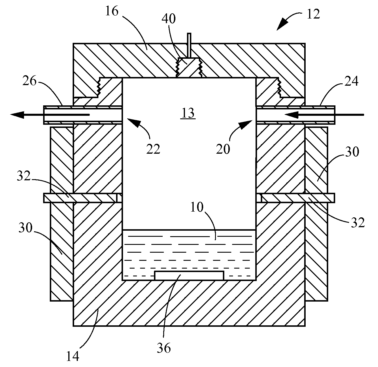
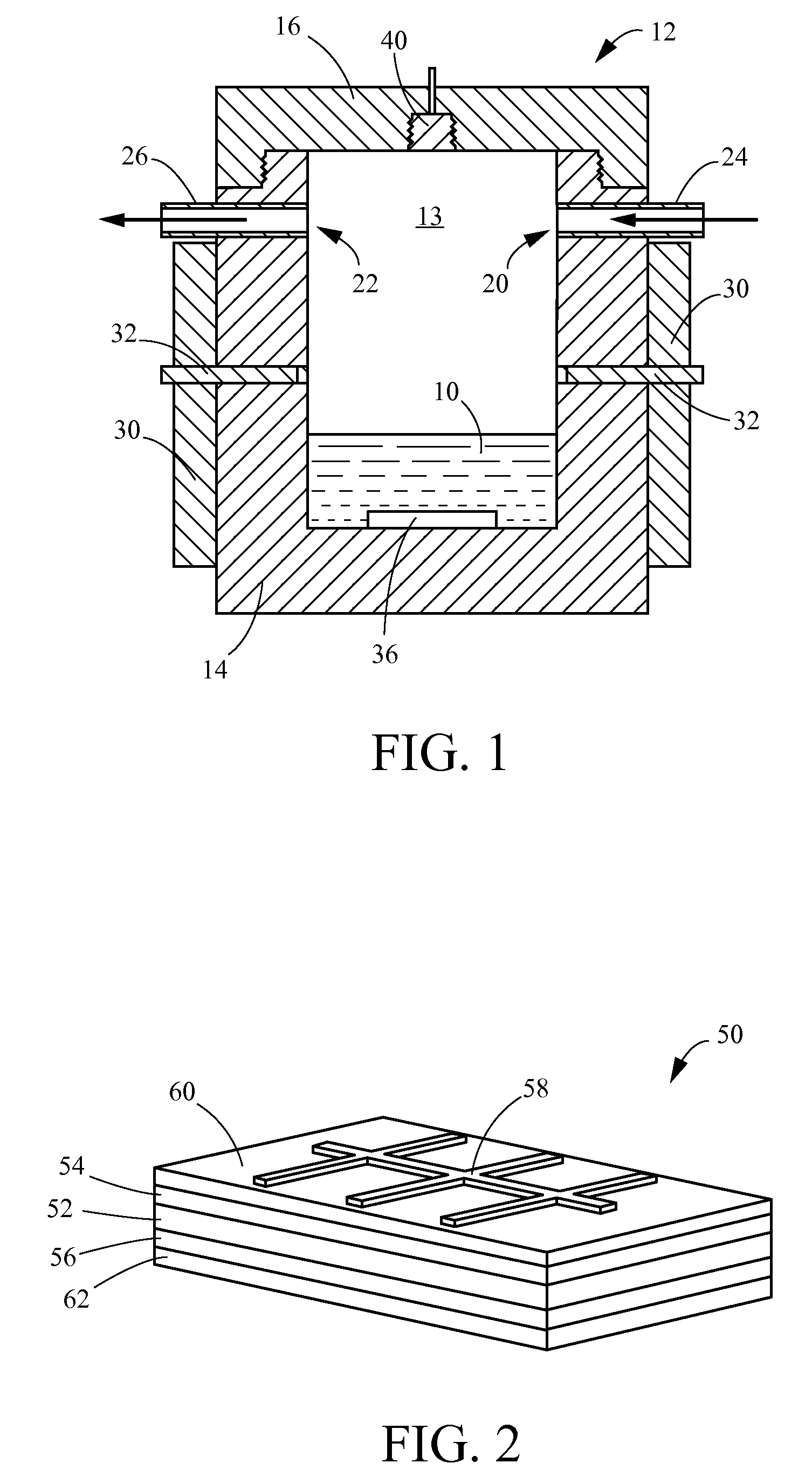
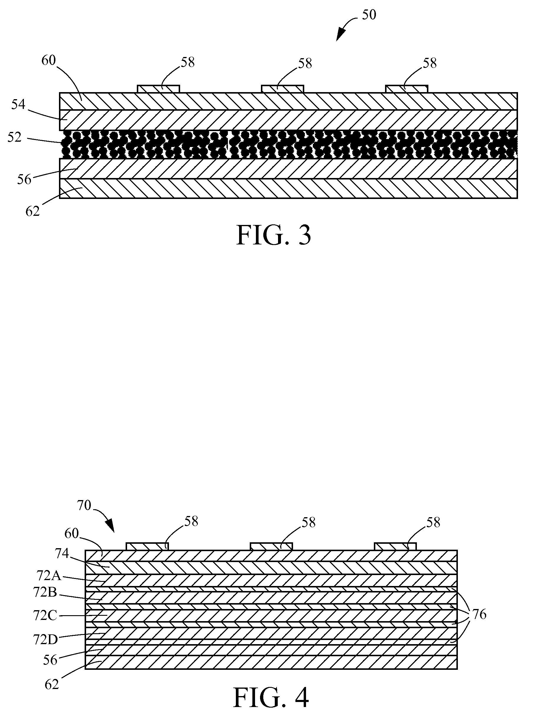
[0021]The illustrations presented herein are not meant to be actual views of any particular apparatus or system, but are merely idealized representations that are employed to describe various embodiments of the present invention. It is noted that elements that are common between figures may retain the same numerical designation.

[0022]As used herein, the term “single source precursor” means and includes any molecule or complex that comprises all of the necessary atomic elements, in the appropriate stoichiometric ratios, necessary to form a ternary chalcopyrite material. Single source precursors may comprise so-called organometallic substances. As non-limiting examples, single source precursors include molecules or complexes having the empirical formula [{L}nM′(ER)x(X)y(R)zM″], wherein x is 1-4, x+y+z=4, L is a Lewis base that is coordinated to M′ by a dative bond, n is greater than or equal to 1, M′ is a Group I-B atom, M″ is a Group III-A atom, E is a Group VI-A atom, X is a group V...


PUM

PropertyMeasurementUnit
Temperatureaaaaaaaaaa
Pressureaaaaaaaaaa
Diameteraaaaaaaaaa

Abstract

Single source precursors are subjected to carbon dioxide to form particles of material. The carbon dioxide may be in a supercritical state. Single source precursors also may be subjected to supercritical fluids other than supercritical carbon dioxide to form particles of material. The methods may be used to form nanoparticles. In some embodiments, the methods are used to form chalcopyrite materials. Devices such as, for example, semiconductor devices may be fabricated that include such particles. Methods of forming semiconductor devices include subjecting single source precursors to carbon dioxide to form particles of semiconductor material, and establishing electrical contact between the particles and an electrode.

Description

GOVERNMENT RIGHTS[0001]The United States Government has certain rights in this invention pursuant to Contract No. DE-AC07-05ID14517 between the United States Department of Energy and Battelle Energy Alliance, LLC.TECHNICAL FIELD[0002]Embodiments of the invention relate to methods for forming particles (e.g., nanoparticles) and to methods for forming semiconductor devices using nanoparticles. Additional embodiments of the invention relate to systems for forming nanoparticles, and to semiconductor devices formed using nanoparticles.BACKGROUND[0003]Semiconductor devices are devices that employ semiconductor materials, which are solid materials that exhibit an electrical conductivity lying between that of a conductor and that of an insulator. Semiconductor devices include, for example, diodes (e.g., light emitting diodes (LEDs)), photovoltaic devices, sensors, solid state lasers, and integrated circuits (e.g., memory modules and microprocessors).[0004]Photovoltaic devices are semiconduc...

Claims


Application Information

Patent Timeline
IPC IPC(8): H01L31/18C08J3/14H01L21/02
CPCH01L21/02485H01L21/02505H01L21/02568H01L21/02601Y10S977/813H01L31/0322Y02E10/541Y10S977/824H01L21/0262
Inventor FOX, ROBERT V.RODRIGUEZ, RENEPAK, JOSHUA
Owner BATTELLE ENERGY ALLIANCE LLC
Why Eureka
Try Eureka