Semiconductor device

a technology of semiconductor devices and capacitors, applied in the direction of semiconductor/solid-state device details, diodes, capacitors, etc., can solve the problems of parasitic capacitance, degrade and the electrical characteristic of a circuit using the capacitance element to become unstable, so as to improve the performance of a semiconductor device

Inactive Publication Date: 2009-09-24
RENESAS ELECTRONICS CORP
View PDF5 Cites 14 Cited by
  • Summary
  • Abstract
  • Description
  • Claims
  • Application Information

AI Technical Summary

Benefits of technology

[0019]An advantage obtained by the representative inventions, among the inventions disclosed in the present application, will be described simply as fo

Problems solved by technology

However, when the dummy pattern of the active region or the gate pattern is disposed below the MIM type capacitance element, since this dummy pattern is an isolated pattern which is not connected to any pattern (so called floating pattern), the dummy pattern has an unstable potential, and thereby sometimes may become a noise sour

Method used


Image

  • Semiconductor device
  • Semiconductor device
  • Semiconductor device

Examples


first embodiment

[0058]A semiconductor device of the present embodiment will be described with reference to the drawings. The semiconductor device of the present embodiment is the one having a capacitance element.

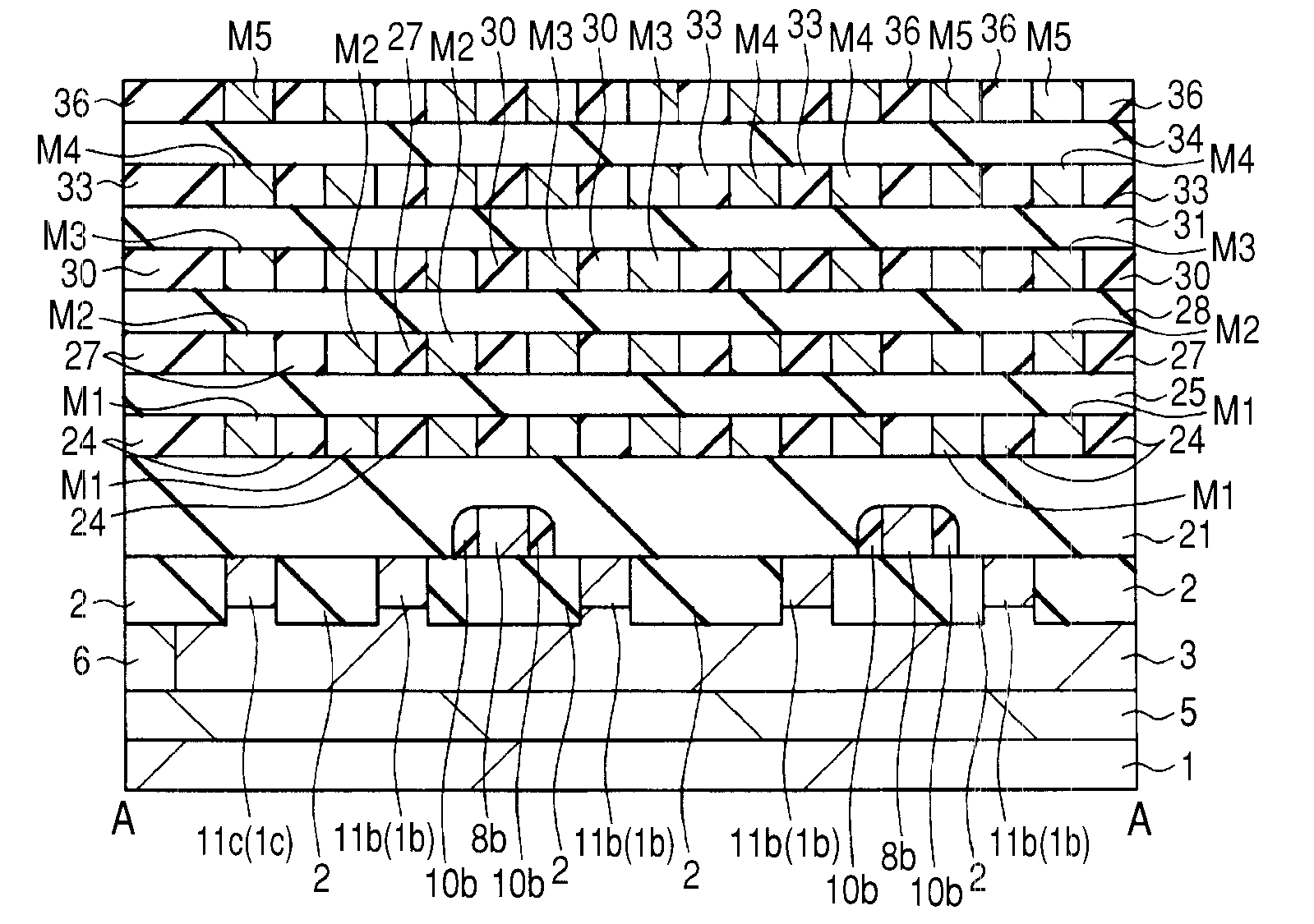
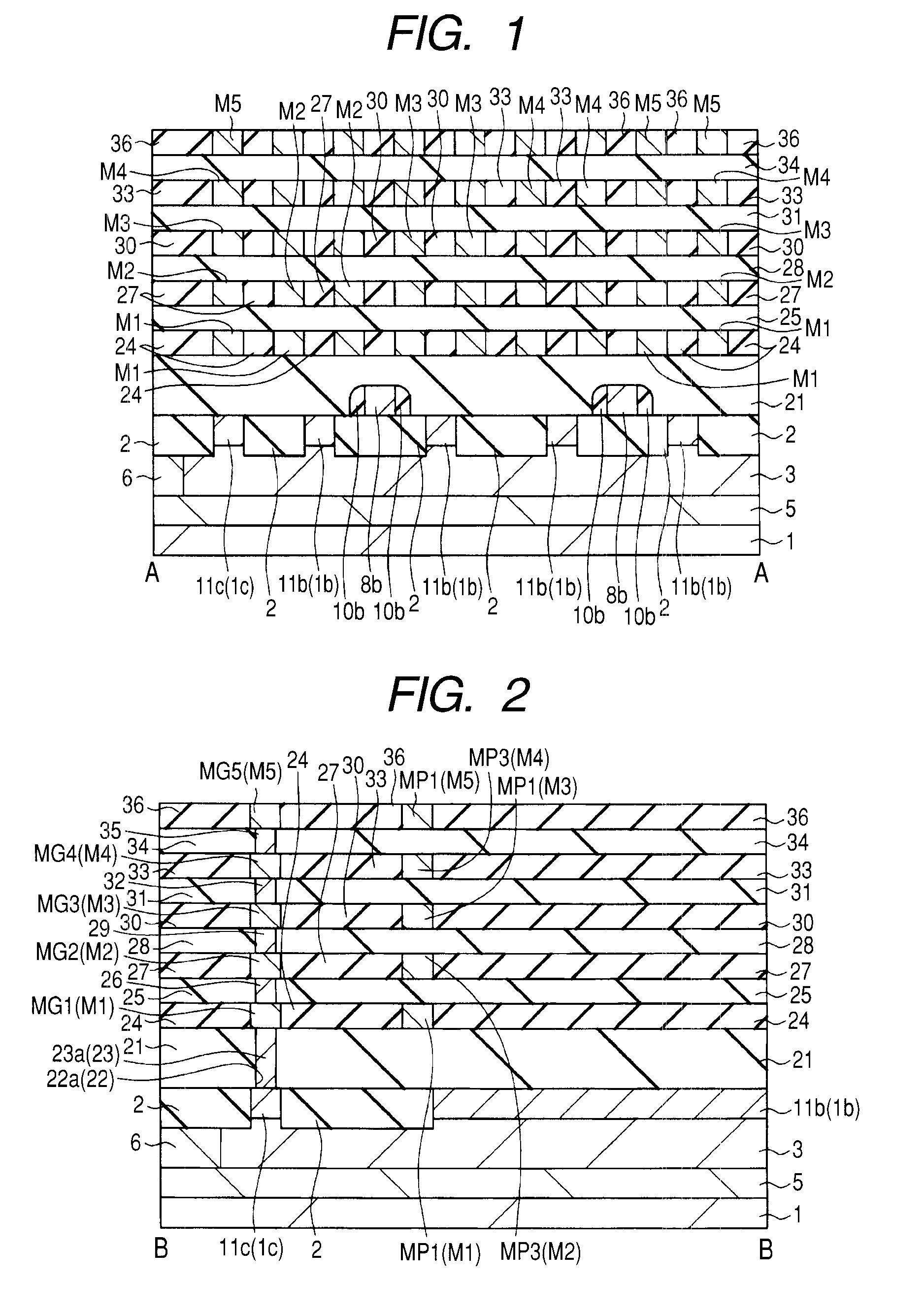
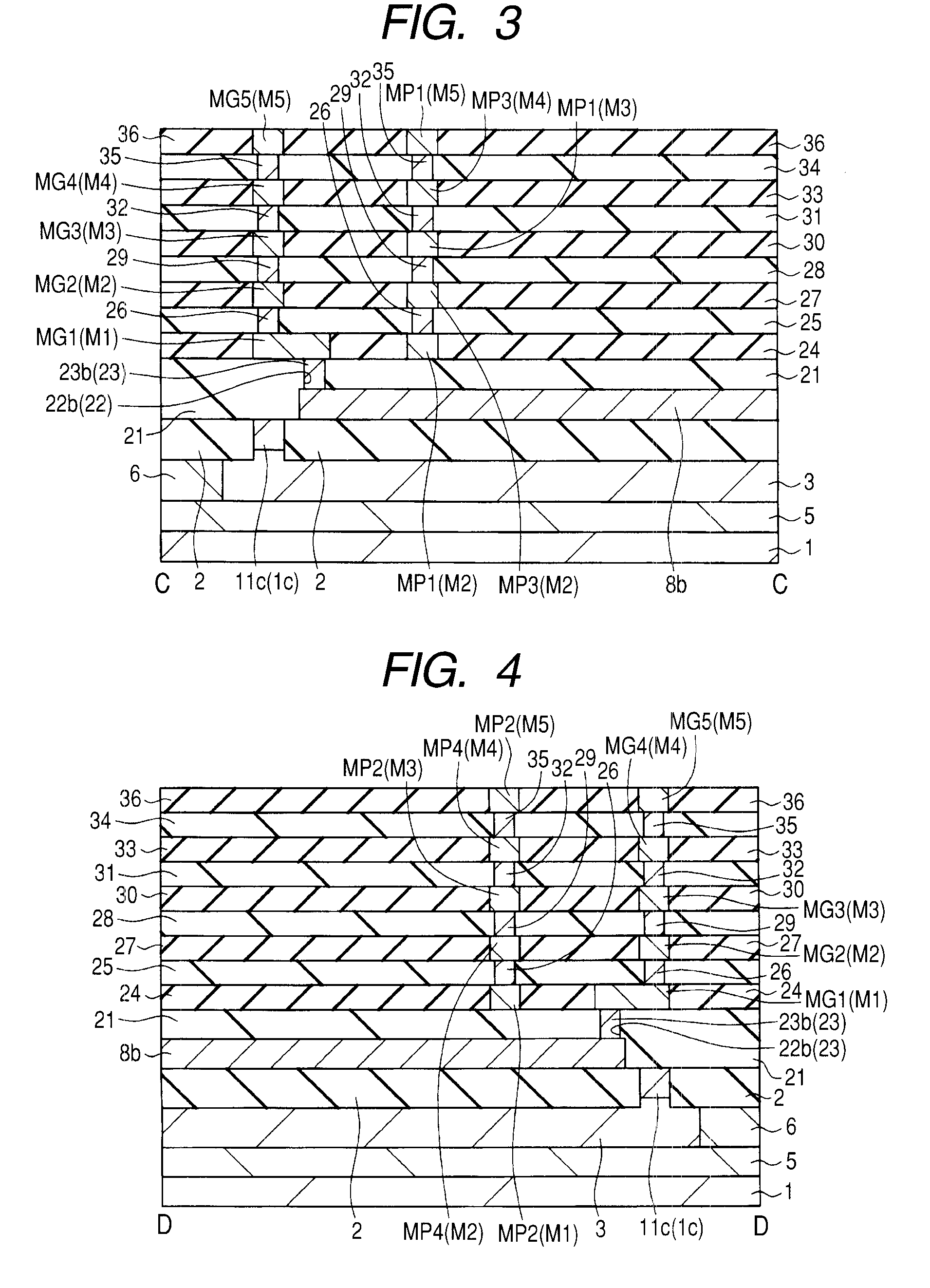
[0059]FIG. 1 to FIG. 7 are cross-sectional views of substantial parts in the semiconductor device of the present embodiment, FIG. 8 to FIG. 18 are plan views of substantial parts in the semiconductor device of the present embodiment. Each of FIG. 1 to FIG. 6 and FIG. 8 to FIG. 18 shows a cross-sectional view or a plan view of a capacitor formation region of the semiconductor device, and FIG. 7 shows a cross-sectional view of a MISFET formation region of the semiconductor device. FIG. 1 corresponds to a cross-section at an A-A line in FIG. 8 or FIG. 9, FIG. 2 corresponds to a cross-section at a B-B line in FIG. 8 or FIG. 9, FIG. 3 corresponds to a cross-section at a C-C line in FIG. 8 or FIG. 9, FIG. 4 corresponds to a cross-section at a D-D line in FIG. 8 or FIG. 9, FIG. 5 corresponds to a ...

second embodiment

[0173]FIG. 31 and FIG. 32 are plan views of substantial parts of the semiconductor device in the present embodiment and correspond to FIG. 15 and FIG. 14 of the above first embodiment, respectively. Note that FIG. 32 is a plan view but provides hatching to the conductor pattern 8b, the p-type semiconductor regions 11b, 11c (active regions 1b, 1c), and the wiring M1 for making the drawings easily to be viewed as in FIG. 14 of the first embodiment.

[0174]Each of the conductor patterns 8b disposed below the capacitance element C1 needs to be electrically coupled to the metal pattern MG1. For this purpose, in the capacitor formation region, each of the conductor patterns 8b needs to cross in a planar manner at least one of the wiring part MC1 in the metal pattern MP1 and the wiring part MC2 in the metal pattern MP2, and to extend in the X direction for being electrically coupled to the metal pattern MG1 via the plug 23b embedded in the contact hole 22b formed in the insulating film 21.

[0...

third embodiment

[0180]FIG. 33 and FIG. 34 are plan views of substantial parts in the semiconductor device of the present embodiment, and correspond to FIG. 31 and FIG. 32 of the above second embodiment, respectively. Note that FIG. 34 is a plan view but provides hatching to the conductor pattern 8b, the p-type semiconductor regions 11b, 11c (active regions 1b, 1c), and the wiring M1 for making the drawings easily to be viewed as in FIG. 14 of the first embodiment and FIG. 32 of the second embodiment.

[0181]Also in the present embodiment, as in the second embodiment, each of the conductor patterns 8b in the capacitor formation region extends in the x direction and is disposed to overlap one of the wiring part MC1 in the metal pattern MP1 and the wiring part MC2 in the metal pattern MP2 in a planar manner, but not to overlap the other one in a planar manner. Then, also in the present embodiment, as in the second embodiment, each of the conductor patterns 8b couples one end thereof, which crosses over ...


PUM


Abstract

To improve a performance of a semiconductor device having a capacitance element. An MIM type capacitance element, an electrode of which is formed with comb-shaped metal patterns composed of the wirings, is formed over a semiconductor substrate. A conductor pattern, which is a dummy gate pattern for preventing dishing in a CMP process, and an active region, which is a dummy active region, are disposed below the capacitance element, and these are coupled to shielding metal patterns composed of the wirings and then connected to a fixed potential. Then, the conductor pattern and the active region are disposed so as not to overlap the comb-shaped metal patterns in the wirings in a planar manner.

Description

CROSS-REFERENCE TO RELATED APPLICATION[0001]The present application claims priority from Japanese patent application No. 2008-68807 filed on Mar. 18, 2008, the content of which is hereby incorporated by reference into this application.BACKGROUND OF THE INVENTION[0002]The present invention relates to a semiconductor device, and particularly to a technique which is effective in an application thereof to a semiconductor device having a capacitance element.[0003]Various semiconductor devices are produced by forming a MISFET, a capacitor, etc. over a semiconductor substrate and by wiring respective elements with wirings. The capacitors formed over the semiconductor substrate include a MOS type capacitance element, a PIP (Poly-silicon Insulator Poly-silicon) type capacitance element, an MIM (Metal Insulator Metal) type capacitance element, etc.[0004]Japanese patent laid-open No. 2005-197396 (Patent document 1) discloses a technique to form a capacitance using a comb-shaped wiring.[0005]Ja...

Claims


Application Information

Patent Timeline
IPC IPC(8): H01L27/06
CPCH01L23/5223H01L27/0207H01L27/0629H01L28/60H01L2924/0002H01L2924/00
Inventor MAEDA, SATOSHISEKINE, YASUSHIWATANABE, TETSUYA
Owner RENESAS ELECTRONICS CORP
Why Eureka
Try Eureka