Liquid crystal device and electronic apparatus

a liquid crystal device and electronic equipment technology, applied in the direction of chemistry apparatus and processes, instruments, transportation and packaging, etc., can solve the problems of weak interaction between liquid crystal molecules, low transmittance, and small effect of improving contrast, so as to prevent the occurrence of display failure, reduce the cost, and avoid the effect of affecting the contras

Inactive Publication Date: 2009-09-24
SEIKO EPSON CORP
View PDF10 Cites 9 Cited by
  • Summary
  • Abstract
  • Description
  • Claims
  • Application Information

AI Technical Summary

Benefits of technology

[0009]An advantage of the invention is to provide a liquid crystal device and an electronic apparatus that show a favorable contrast characteristic by preventing occurrence of a display failure such as a disclination and reduce the cost.
[0010]A liquid crystal device according to a first aspect of the invention includes: a circuit substrate; a counter substrate disposed so as to be opposed to the circuit substrate; a liquid crystal layer sandwiched between the circuit substrate and the counter substrate, the liquid crystal layer showing vertical alignment as an initial alignment state; a first alignment layer manufactured on a side of the counter substrate using a coating process, the side facing the liquid crystal layer, the first alignment layer having a vertical alignment function; and a second alignment layer manufactured on a side of the circuit substrate using a vacuum deposition process, the side facing the liquid crystal layer, the second alignment layer generating a pretilt.
[0011]By adopting the first aspect of the invention, the coating-type (coating process) first alignment layer is provided on the counter substrate of the substrates forming a pair. This do not need for manufacturing alignment layers on the two substrates using a vacuum deposition process (oblique evaporation) when a liquid crystal device is mass-produced, thereby reducing the number of expensive vacuum deposition systems. As a result, initial investment cost is significantly reduced. Also, since the second alignment layer made by the method of an oblique evaporated is provided on the circuit substrate, the alignment direction in which liquid crystal molecules are tilted when applying a voltage is controlled. Consequently, the liquid crystal molecules are tilted in one direction by suppressing the influences of a lateral electric field generated out of the pixel electrode, thereby effectively preventing occurrence of a disclination. As a result, a liquid crystal display having high display quality is manufactured at low cost.
[0012]In the liquid crystal device according to the first aspect of the invention, a pretilt angle generated by the second alignment layer is preferably in the range of 81.0° to 86.5°.
[0013]By adopting the first aspect of the invention, the pretilt angle is in the range of 81.0° to 86.5°. This prevents a lateral electric field from affecting conflict between the liquid crystal molecules, thereby maintaining a high-contrast characteristic while preventing occurrence of a disclination. If the pretilt angle on the second alignment layer is smaller than 81.0°, the liquid crystal molecules are tilted more than necessary when applying no voltage. This causes a deterioration in contrast. If the pretilt angle on the second alignment layer is larger than 86.5°, it is difficult to control the direction in which the liquid crystal molecules are aligned when applying a voltage.
[0014]An electronic apparatus according to a second aspect of the invention includes the liquid crystal device according to the first aspect of the invention.

Problems solved by technology

However, since liquid crystal molecules are aligned vertically to surfaces of substrates in the vertical alignment mode, interactions between the liquid crystal molecules are weak in the azimuth direction in which the liquid crystal molecules are tilted when applying a voltage.
Also, since some liquid crystal molecules do not contribute to display depending on the azimuth (that is, liquid crystal molecules parallel with the transmission axis of any one of polarizing plates under the crossed nicols condition do not make a phase difference), there occurs a problem that the transmittance becomes lower than that in parallel alignment.
However, a substantial average tilt angle for preventing a lateral electric field from affecting the alignment is almost the same as a pretilt angle used under mass-production conditions so that little effect for improving the contrast is obtained.
Also, alignment layers provided on the opposed surfaces of the two substrates are manufactured by oblique evaporation, and if a liquid crystal device is mass-produced, multiple expensive apparatuses such as vacuum deposition systems are required.
However, it is difficult to tilt liquid crystal molecules from a completely vertical state by performing rubbing on polyimide for vertical alignment that can be used as a coating.
As for this method, a disclination attributable to competition between liquid crystal molecules almost always occurs in each pixel; however, such a disclination is not remarkable, since the size of each pixel is several tens of micron meter.
Nevertheless, a liquid crystal panel, such as HTPS (high temperature poly-silicon) or LCOS (liquid crystal on silicon), that is used as a light valve of a projector and whose pixel size is around 10 μm has a problem that a disclination can be visually recognized during projection so that display quality is degraded.
This causes a deterioration in contrast.
If the pretilt angle on the second alignment layer is larger than 86.5°, it is difficult to control the direction in which the liquid crystal molecules are aligned when applying a voltage.

Method used


Image

  • Liquid crystal device and electronic apparatus
  • Liquid crystal device and electronic apparatus
  • Liquid crystal device and electronic apparatus

Examples


example 1

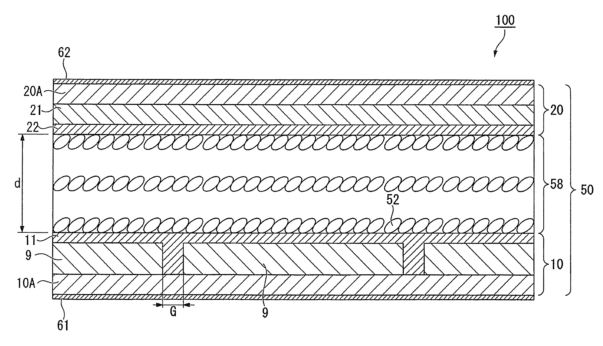
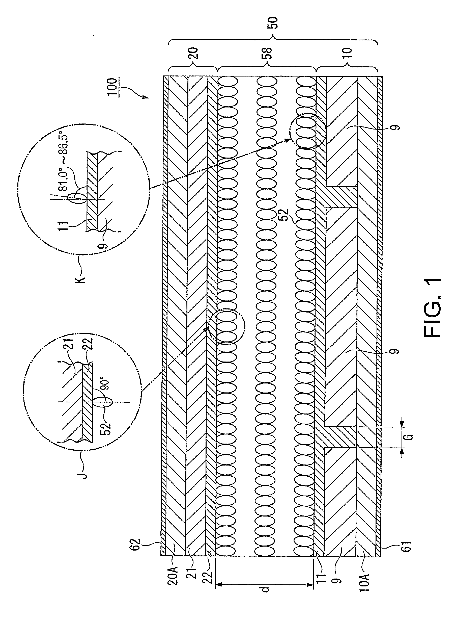
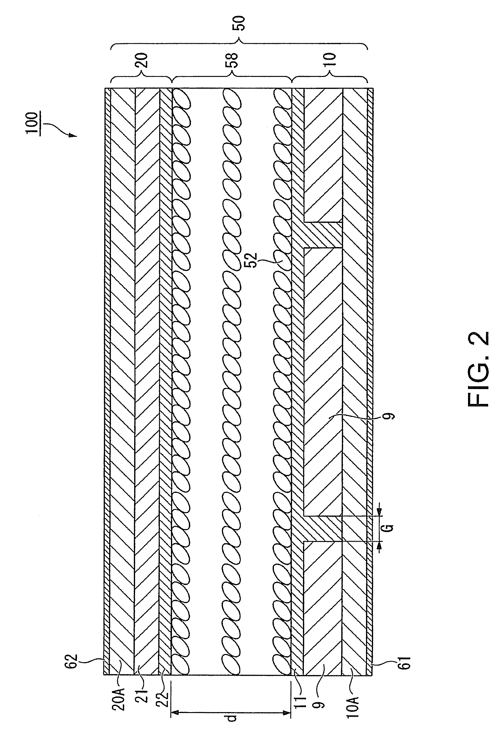
[0045]Pretilt was generated on the circuit substrate 10 by the second alignment layer 11 manufactured using a known method such as oblique evaporation. In this example, a substrate was set in such a manner that the substrate is tilted with respect to an evaporation source by a certain angle θ and then SiO2 was evaporated onto the substrate. The second alignment layer 11 has a function (pretilt) of aligning the liquid crystal molecules 52 at an angle of 82.0° with respect to the substrate surface.

[0046]As for the counter substrate 20, an organic PI material was applied to a surface of the common electrode 21 using a method such as spin-coating or flexography so that the first alignment layer 22 is manufactured. The first alignment layer 22 is intended to align the liquid crystal molecules 52 at an angle of approximately 90° with respect to the substrate surface.

[0047]The circuit substrate 10 and counter substrate 20 manufactured as described above were combined together via a sealant...


PUM

PropertyMeasurementUnit
pretilt angleaaaaaaaaaa
sizeaaaaaaaaaa
pretilt angleaaaaaaaaaa

Abstract

A liquid crystal device includes: a circuit substrate; a counter substrate disposed so as to be opposed to the circuit substrate; a liquid crystal layer interposed between the circuit substrate and the counter substrate, the liquid crystal layer showing vertical alignment as an initial alignment state; a first alignment layer manufactured on a side of the counter substrate using a coating process, the side facing the liquid crystal layer, the first alignment layer having a vertical alignment function; and a second alignment layer manufactured on a side of the circuit substrate using a vacuum process, the side facing the liquid crystal layer, the second alignment layer generating a pretilt.

Description

CROSS-REFERENCE TO RELATED APPLICATION[0001]This application is based on and claims priority from Japanese Patent Application No. 2008-069223, filed on Mar. 18, 2008, the contents of which are incorporated herein by reference.BACKGROUND[0002]1. Technical Field[0003]The present invention relates to a liquid crystal device and an electronic apparatus.[0004]2. Related Art[0005]In recent years, the vertical alignment mode has been adopted as the mode of aligning liquid crystal in a liquid crystal device for use in a projector. However, since liquid crystal molecules are aligned vertically to surfaces of substrates in the vertical alignment mode, interactions between the liquid crystal molecules are weak in the azimuth direction in which the liquid crystal molecules are tilted when applying a voltage. Accordingly, when applying a voltage, the liquid crystal molecules are tilted in various directions due to a lateral electric field that occurs from an electrode edge. Also, since some liqu...

Claims


Application Information

Patent Timeline
Patent Type & Authority Applications(United States)
IPC IPC(8): G02F1/1337
CPCG02F1/133723G02F1/133734Y10T428/1018G02F2001/133746Y10T428/1023G02F2001/13373C09K2323/025C09K2323/027G02F1/13373G02F1/133746
Inventor NAGAE, NOBUKAZUMIYASHITA, TAKESHI
Owner SEIKO EPSON CORP
Why Eureka
Try Eureka