Semiconductor integrated circuit and design automation system

a technology of integrated circuit and design automation system, applied in the direction of program control, instruments, error detection/correction, etc., can solve the problems of insufficient countermeasures in restraining instantaneous power, inability to reduce power consumption, and inability to achieve instantaneous power

Inactive Publication Date: 2009-09-24
KK TOSHIBA
View PDF20 Cites 30 Cited by
  • Summary
  • Abstract
  • Description
  • Claims
  • Application Information

AI Technical Summary

Benefits of technology

[0013]Furthermore, another aspect of the present invention provides a semiconductor integrated circuit, comprising: a combinational logic circuit; a scan chain circuit comprising a plurality of flip-flops that are serially connected, and configured to temporarily store data that is inputted to and outputted from the combinational logic circuit during ordinary operation, and to cause the plurality of flip-flops to function as shift registers to execute a scan shift that serially transfers test pattern data for a scan test during execution of a scan test; and a clock gating circuit configured to control output of a pulse of a clock signal supplied to the scan chain circuit in accordance with a clock gating signal, whereas disab...

Problems solved by technology

Therefore, power consumption may become a problem (see, for example, P. Girad, “Survey of Low-Power Testing of VLSI Circuits,” IEEE Design & Test of Computers, Vol. 19, No. 3, pp.
However, since all the scan F/Fs operate simultaneously, this is an insufficient countermeasure in restraining instantaneous power.
However, in the case that there exists a main clock domain extending ...

Method used


Image

  • Semiconductor integrated circuit and design automation system
  • Semiconductor integrated circuit and design automation system
  • Semiconductor integrated circuit and design automation system

Examples


first embodiment

[0028]A semiconductor integrated circuit according to a first embodiment of the present invention is described with reference to the drawings.

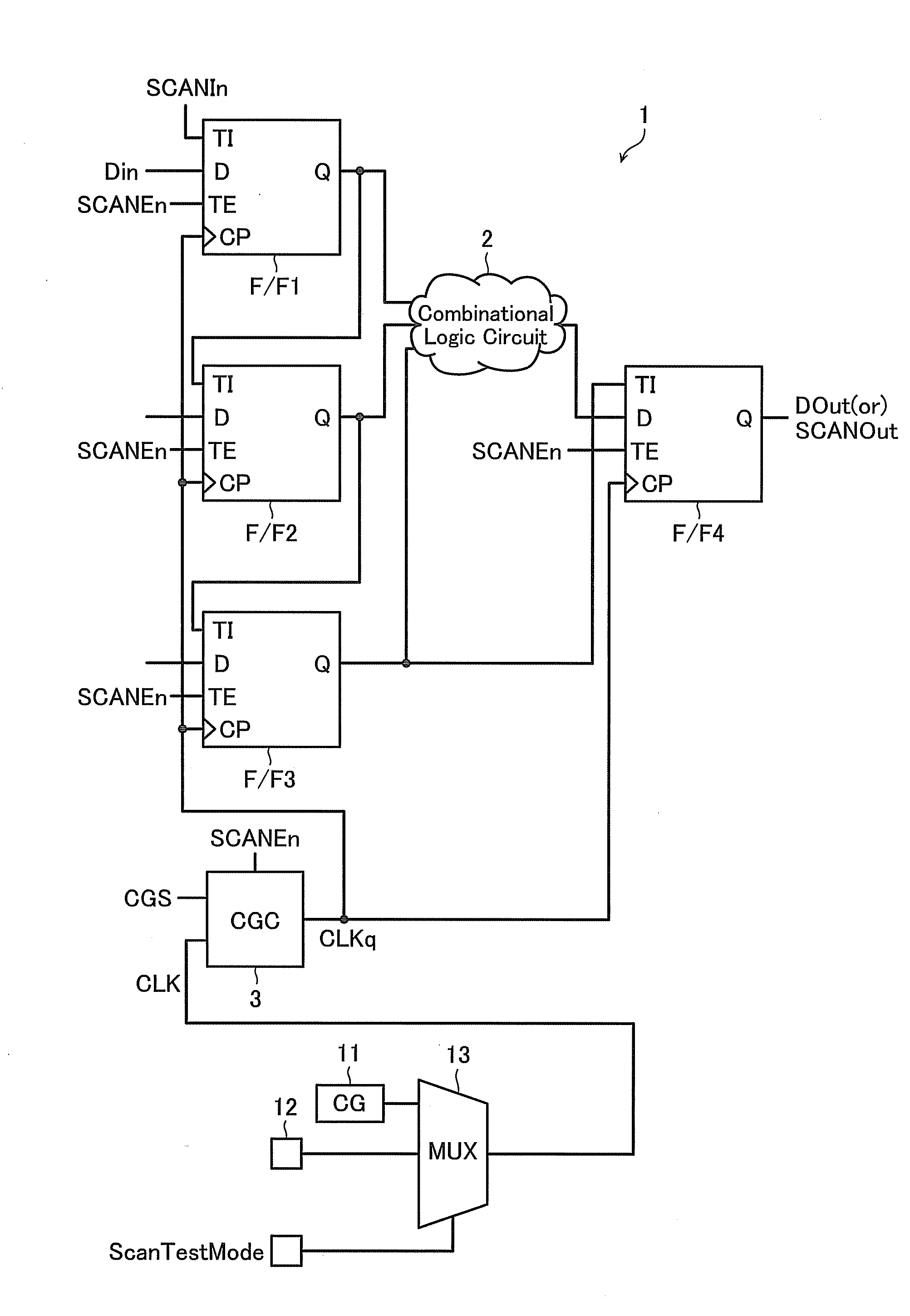
[0029]Prior to description of the first embodiment, an example of a configuration of a general scan chain circuit and combinational logic circuit is explained with reference to FIG. 1. A combinational logic circuit 2 has scantest flip-flops F / F1 to F / F3 disposed on an input terminal side thereof and scantest flip-flop F / F4 disposed on an output terminal side thereof. In addition, these four flip-flops F / F1 to F / F4 are connected in series to constitute a scan chain circuit 1 functioning as a shift register during a scan test.

[0030]That is to say, in ordinary operation, these flip-flops F / F1 to F / F3 temporarily store input data Din inputted to them through data input terminals D, and output output data to the combinational logic circuit 2 through data output terminals Q. In addition, flip-flop F / F4 temporarily stores data outputted from the comb...

second embodiment

[0055]Next, a design automation system according to a second embodiment of the present invention is described with reference to the drawings.

[0056]FIG. 7 is a block diagram showing a configuration of a design automation system in accordance with a second embodiment of the present invention. This design automation system is realizable through a computer and a computer program, and in one example is provided with a netlist storage unit 41 that stores a netlist of the semiconductor integrated circuit to be designed, a circuit design unit 42, and an output unit 43.

[0057]Here, a netlist stored in the netlist storage unit 41 is to include combinational logic circuits, flip-flops, and clock gating circuits.

[0058]The circuit design unit 42 is provided with a counting section 401, a selecting section 402, a substituting section 403, a judging section 404, and a netlist generating section 405. 401 to 405 are realizable also by way of the computer program that is stored in and executed by the ...

third embodiment

[0068]Next, a design automation system according to a third embodiment of the present invention is described with reference to the drawings.

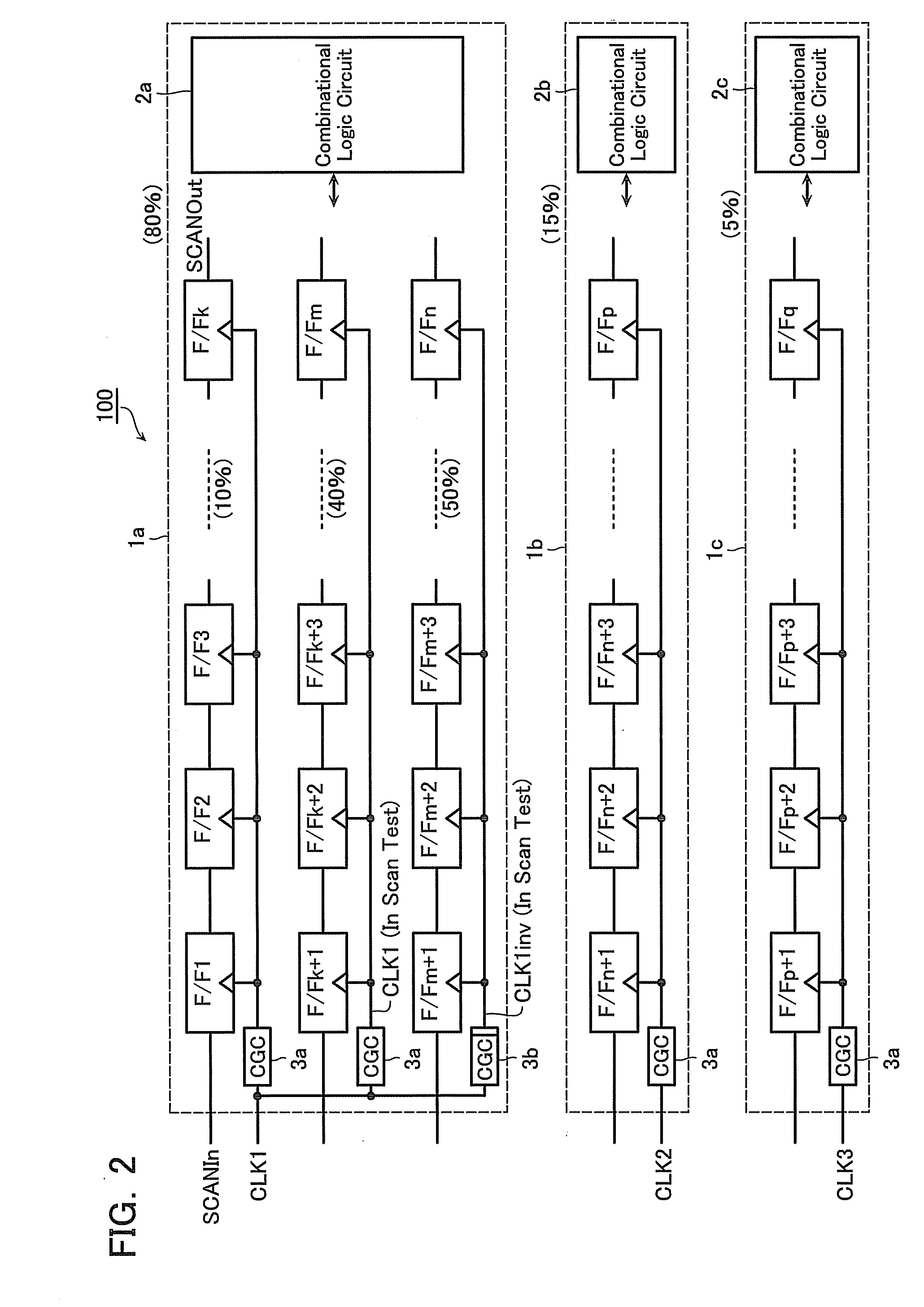
[0069]FIG. 10 is a block diagram showing a configuration of a design automation system in accordance with a third embodiment of the present invention. This design automation system is realizable through a computer and a computer program, and in one example is configured so as to enable automatic design of a semiconductor integrated circuit such as that shown in FIG. 2. The system is configured from an input unit 141, a data storage section 142, a netlist generating section 143, a test pattern generating section 144, and an output section 145. The sections 143 to 144 are realizable also by way of the computer program that is stored in and executed by the computer.

[0070]The input unit 141 is provided to input a selection for inverted clocking described below and other instructions from an operator necessary for the design. The data storage section...


PUM


Abstract

A scan chain circuit causes a plurality of flip-flops to function as shift registers during execution of a scan test and can execute a scan shift that serially transfers test pattern data for the scan test. A clock gating circuit controls output of a pulse of a clock signal supplied to the scan chain circuit in accordance with a clock gating signal, whereas disables the clock gating signal based on a logic of a scan enable signal authorizing the scan shift. A first clock gating circuit included in the clock gating circuit disables the clock gating signal during the scan shift based on the logic of the scan enable signal and also inverts the clock signal and outputs a result of inverting.

Description

CROSS REFERENCE TO RELATED APPLICATION[0001]This application is based on and claims the benefit of priority from prior Japanese Patent Application No. 2008-69216, filed on Mar. 18, 2008, the entire contents of which are incorporated herein by reference.BACKGROUND OF THE INVENTION[0002]1. Field of the Invention[0003]The present invention relates to a semiconductor integrated circuit and a design automation system that automates design of a semiconductor integrated circuit.[0004]2. Description of the Related Art[0005]To test whether or not a semiconductor integrated circuit (hereafter referred to as “LSI”) has been manufactured normally, a scan test method is generally used. A scan test is executed by substituting flip-flops (for convenience, “flip-flop” is hereafter referred to as “F / F”) within an LSI by F / Fs having input / output terminals for a scan test called scan F / Fs. A plurality of such scan F / Fs are connected in series to form a scan chain structure within the LSI and a test pa...

Claims


Application Information

Patent Timeline
IPC IPC(8): G01R31/3177G06F11/25
CPCG01R31/31727
Inventor HASEGAWA, TETSU
Owner KK TOSHIBA
Why Eureka
Try Eureka