Method of forming a cobalt metal nitride barrier film

Inactive Publication Date: 2009-10-01
TOKYO ELECTRON LTD
View PDF44 Cites 95 Cited by
  • Summary
  • Abstract
  • Description
  • Claims
  • Application Information

AI Technical Summary

Benefits of technology

[0006]A method is provided for forming a cobalt metal nitride barrier film on a substrate for semiconductor devices. The addition of cobalt (Co) into a metal nitride layer can remove grain bo

Problems solved by technology

The use of a low resistivity metal such as copper (Cu) provides significant gains in switching delay (RC-delay) and power consumption of integrated circuits.
Cu metal cannot be put in direct contact with dielectric materials since Cu metal has poor adhesion to the dielectric materials and Cu metal is known to easily diffuse into common integrated circuit materials such as silicon and dielectric materials where Cu metal is a

Method used


Image

  • Method of forming a cobalt metal nitride barrier film
  • Method of forming a cobalt metal nitride barrier film
  • Method of forming a cobalt metal nitride barrier film

Examples


Embodiment Construction

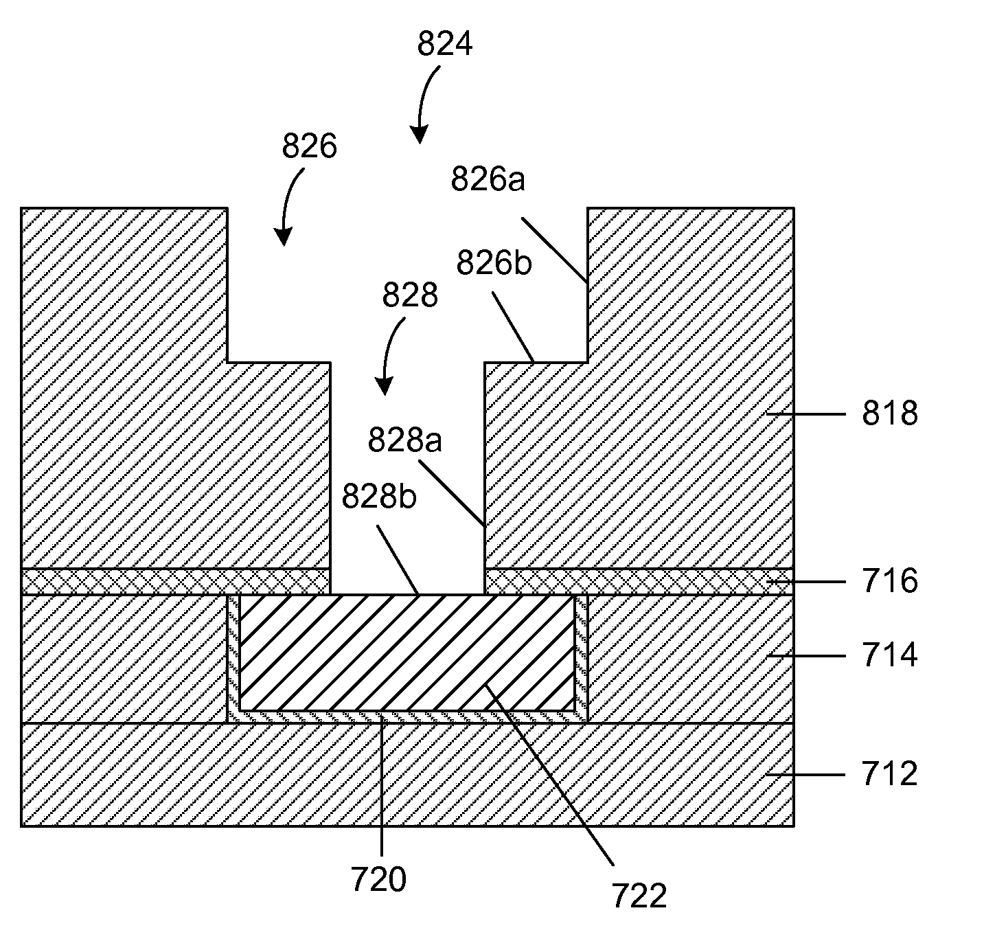
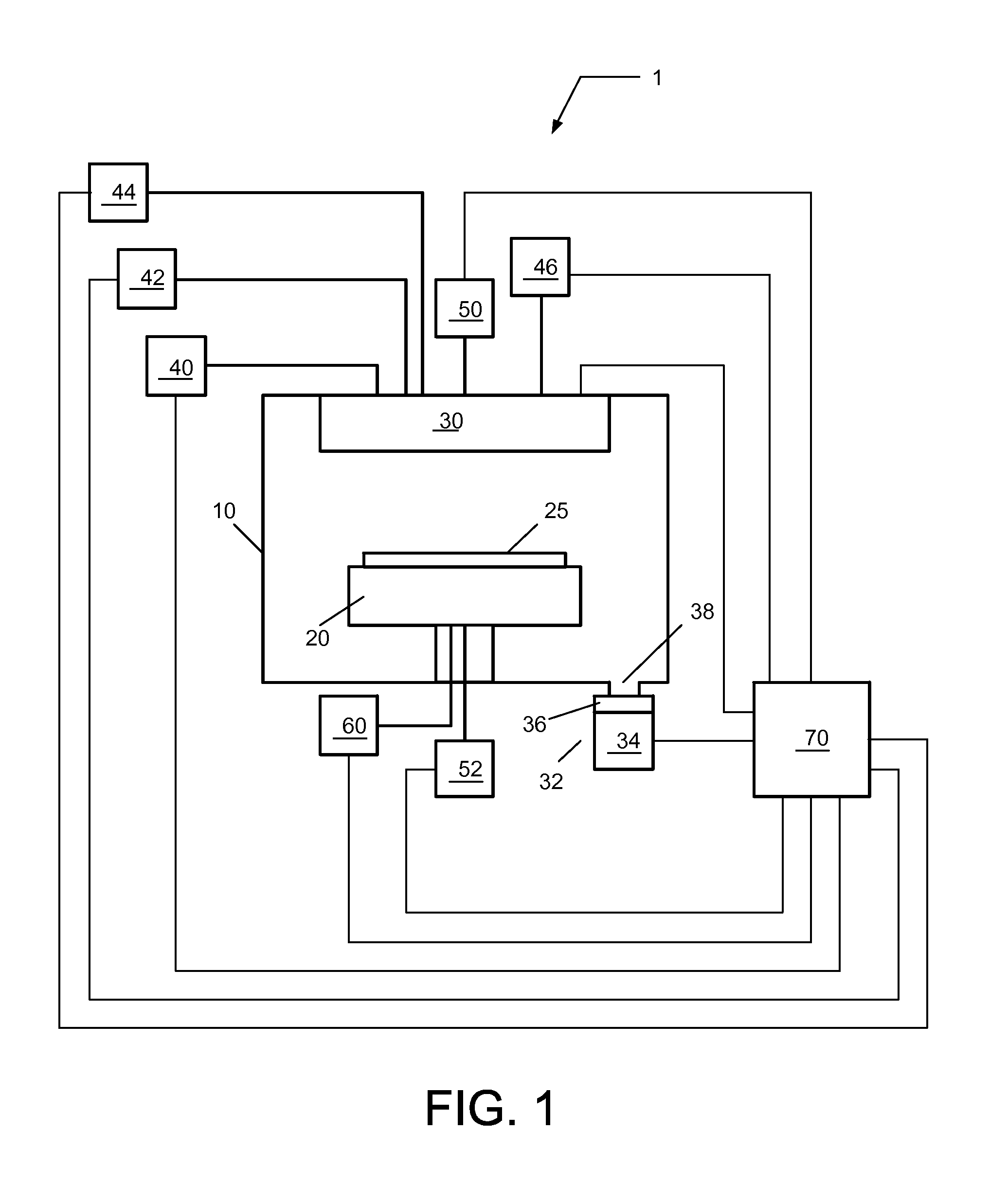
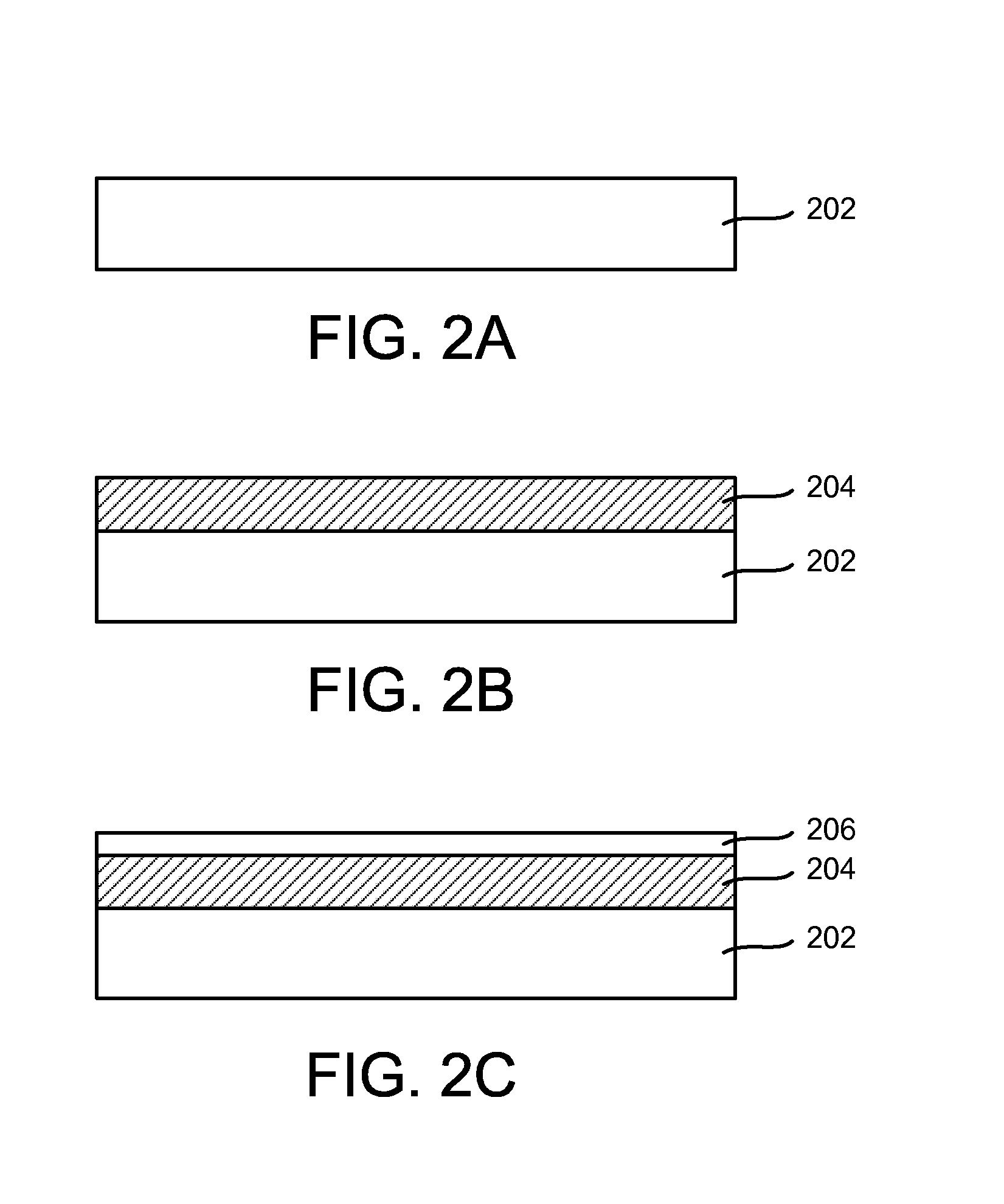
[0019]Formation of cobalt metal nitride barrier films that may be utilized in Cu metallization for semiconductor devices is disclosed in various embodiments. The cobalt metal nitride barrier film may be formed over a surface of recessed feature in a dielectric layer where the recessed feature may have an exposed metallization layer at the bottom of the recessed feature. According to embodiments of the invention, intermixing of cobalt and metal nitride in the cobalt metal nitride film reduces or prevents polycrystalline or columnar film growth and forms a substantially amorphous structure that provides improved diffusion barrier properties against oxygen, Cu, and Si diffusion, for example. The cobalt metal barrier film can further provide lower electrical resistance compared to the corresponding metal nitride material which results in significant gains in switching delay (RC-delay) and power dissipation in the integrated circuit. Furthermore, the cobalt metal nitride barrier film can...


PUM

PropertyMeasurementUnit
Temperatureaaaaaaaaaa
Percent by atomaaaaaaaaaa

Abstract

A method is provided for forming a cobalt metal nitride barrier film on a substrate for semiconductor devices. According to one embodiment of the invention, the method includes depositing a plurality of metal nitride layers on the substrate, and depositing a cobalt layer between each of the plurality of metal nitride layers. According to another embodiment of the invention, the method includes simultaneously exposing the substrate to a metal nitride precursor or a metal precursor, a cobalt precursor, and a reducing gas, nitriding gas, or a combination thereof. Embodiments for integrating a cobalt metal nitride barrier film into semiconductor devices are described.

Description

CROSS-REFERENCE TO RELATED APPLICATIONS[0001]This application is related to co-pending U.S. patent application Ser. No. 11 / 839,410, entitled “SEMICONDUCTOR DEVICE CONTAINING AN ALUMINUM TANTALUM CARBONITRIDE BARRIER FILM AND METHOD OF FORMING,” filed on Aug. 15, 2007, the entire content of which is hereby incorporated by reference.FIELD OF INVENTION[0002]The field of the invention relates generally to the field of forming a semiconductor device, and more specifically to the use of a cobalt metal barrier film for copper metallization.BACKGROUND OF THE INVENTION[0003]An integrated circuit contains various semiconductor devices and a plurality of conducting metal paths that provide electrical power to the semiconductor devices and allow these semiconductor devices to share and exchange information. Within a semiconductor device, metal layers are stacked on top of one another using intermetal or interlayer dielectric layers that insulate the metal layers from each other. Metal layers ty...

Claims


Application Information

Patent Timeline
IPC IPC(8): H01L21/768
CPCC23C16/34H01L21/28562H01L21/76843H01L21/76844H01L21/76846H01L21/76849H01L21/76873H01L2924/0002H01L23/53238H01L2221/1089H01L2924/3011H01L2924/00
Inventor ISHIZAKA, TADAHIROMIZUNO, SHIGERU
Owner TOKYO ELECTRON LTD
Why Eureka
Try Eureka