Method for manufacturing a circuit board having an embedded component therein
a technology of embedded components and circuit boards, which is applied in the manufacturing of contact members, printed circuit aspects, and semiconductor/solid-state device details. it can solve the problems of conventional circuit boards that cannot meet the requirements of light, thin, short and small products, and the thickness of the whole circuit board cannot be increased, so as to reduce the thickness of the embedded component electrodes
- Summary
- Abstract
- Description
- Claims
- Application Information
AI Technical Summary
Benefits of technology
Problems solved by technology
Method used
Image
Examples
first embodiment
[0029]Referring to FIG. 8, it depicts a method for manufacturing a circuit board having an embedded component therein according to the present invention. Referring to FIG. 9, in the step 402 a core layer 510 is provided, wherein the core layer 510 includes a first dielectric layer 512, and first and second metallic layers 514, 516. The first dielectric layer 512 has an upper surface 512a and a lower surface 512b, the first and second metallic layers 514, 516 are located on the upper surface 512a and the lower surface 512b of the first dielectric layer 512 respectively. In this embodiment, the first and second metallic layers 514, 516 are made of copper (Cu) and have a thickness being equal to or less than 3 micrometer (μm).
[0030]Referring to FIG. 10, in the step 404 a first through hole 511 is formed in the core layer 510. For example, the first through hole 511 can be formed in the core layer 510 by mechanic drilling process or laser drilling process. In this embodiment, at least o...
second embodiment
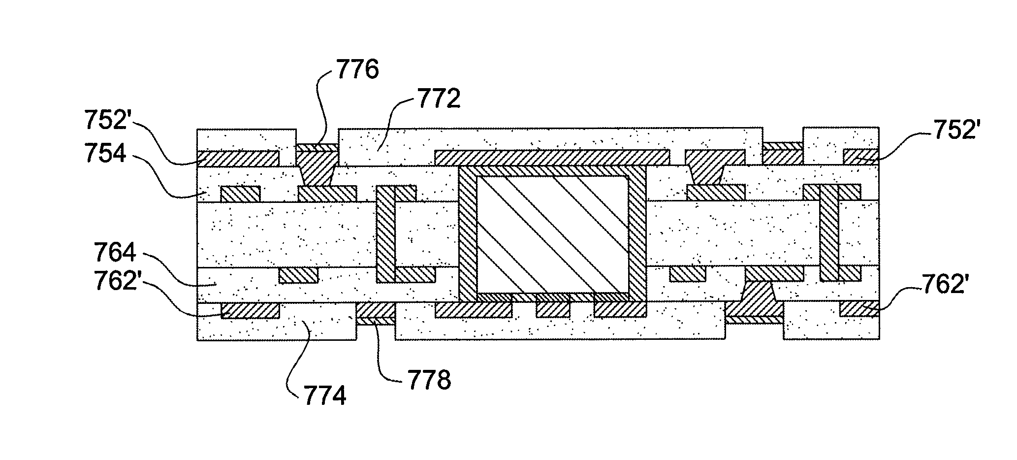
[0041]Referring to FIG. 19, it depicts a method for manufacturing a circuit board having an embedded component therein according to the present invention. Referring to FIG. 20, in the step 602 a core layer 710 is provided, wherein the core layer 710 includes first, second and third dielectric layers 712, 754, 764, first and second patterned circuit layers 742′, 744′, and at least one first conductive via 746. The first dielectric layer 712 has an upper surface 712a and a lower surface 712b, and the first and second patterned circuit layers 742′, 744′ are located on the upper surface 712a and the lower surface 712b of the first dielectric layer 712 respectively. The second dielectric layer 754 is disposed on the upper surface 712a of the first dielectric layer 712, and covers the first patterned circuit layer 742′. The third dielectric layer 764 is disposed on the lower surface 712b of the first dielectric layer 712, and covers the second patterned circuit layer 744′. The first condu...
PUM
| Property | Measurement | Unit |
|---|---|---|
| thickness | aaaaa | aaaaa |
| thickness | aaaaa | aaaaa |
| thickness | aaaaa | aaaaa |
Abstract
Description
Claims
Application Information


