Method of detecting heavy metal in semiconductor substrate

a technology of heavy metal and semiconductor substrate, which is applied in the testing/measurement of individual semiconductor devices, semiconductor/solid-state devices, instruments, etc., can solve the problems of reducing the proportion of devices with good quality, reducing strength, and reducing the technique for detecting heavy metal in thin substrates. , to achieve the effect of improving the certainty of gettingtering capability and reducing the proportion of defective devices

Active Publication Date: 2009-10-15
SUMCO CORP
View PDF9 Cites 4 Cited by
  • Summary
  • Abstract
  • Description
  • Claims
  • Application Information

AI Technical Summary

Benefits of technology

[0017]4. To enable manufacturing of a semiconductor substrate with improved certainty of a gettering capability.
[0018]5. To clarify the cause of device defects by detecting ...

Problems solved by technology

In addition, the heavy metal contamination mostly occurs during the thinning process that is the final step of the device manufacturing process, and therefore there is a problem in that the proportion of devices with good quality is reduced by the heavy metal contamination during the thinning process.
However, since handling of the thin substrate subjected to the thinning process is different from that of a silicon substrate having a thickness of 700 to 1000 μm, a technique for detecting heavy metal in a thin substrate has not been established yet.
Particularly, reduction in strength caused by the thinning process, dif...

Method used


Image

  • Method of detecting heavy metal in semiconductor substrate
  • Method of detecting heavy metal in semiconductor substrate
  • Method of detecting heavy metal in semiconductor substrate

Examples


Embodiment Construction

[0031]Hereinafter, a method of detecting heavy metal in a semiconductor substrate according to an embodiment of the invention will be described with reference to the accompanying drawings.

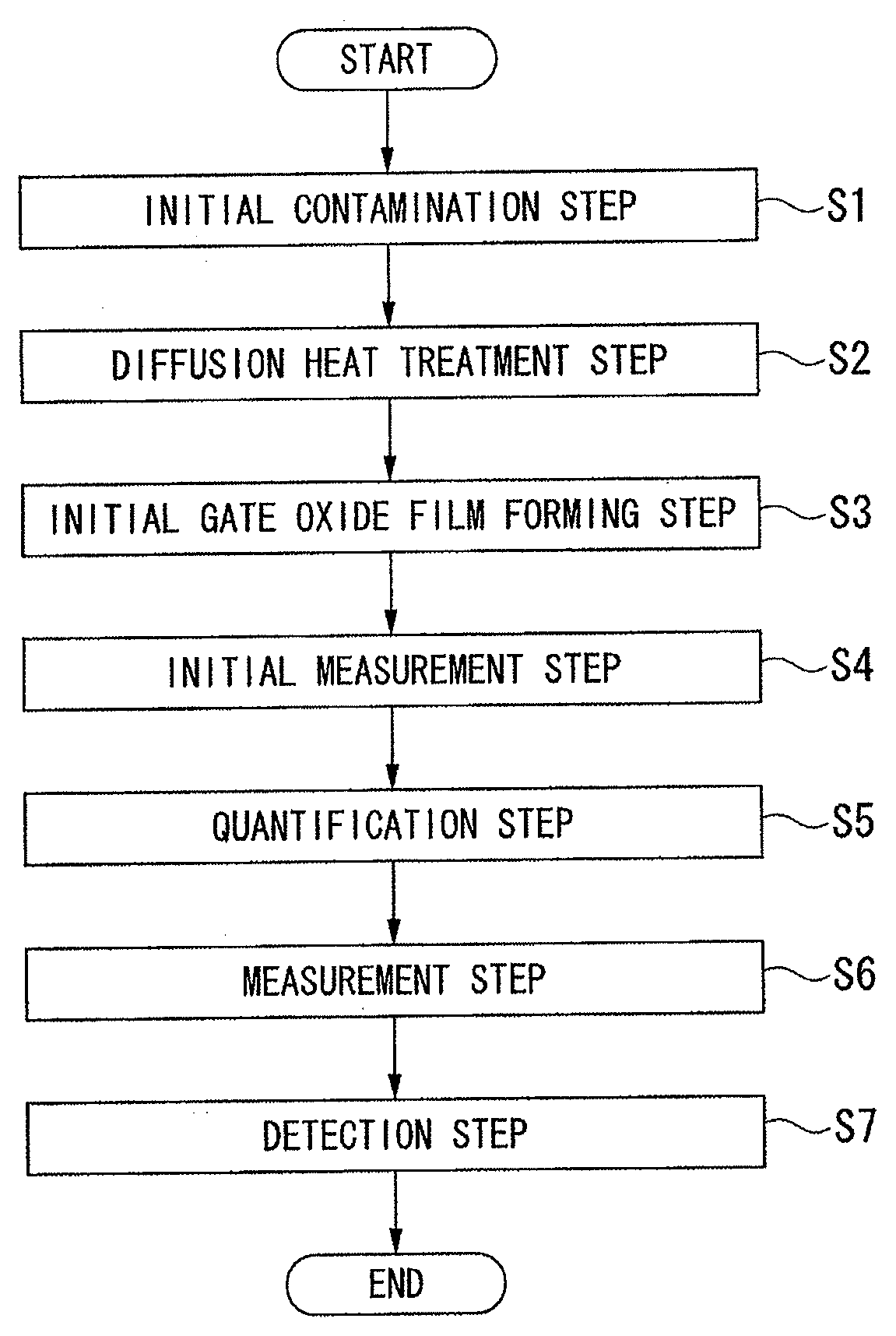
[0032]FIG. 1 is a flowchart illustrating the method of detecting heavy metal in a semiconductor substrate according to the embodiment.

[0033]According to the embodiment, as illustrated in FIG. 1, the method includes an initial contamination step S1, a diffusion heat treatment step S2, an initial gate oxide film forming step S3, an initial measurement step S4, a quantification step S5, a measurement step S6, and a detection step S7. It is possible to give appropriate modification in these steps, such as changing the order of steps or omitting the step(s), depending on the purpose.

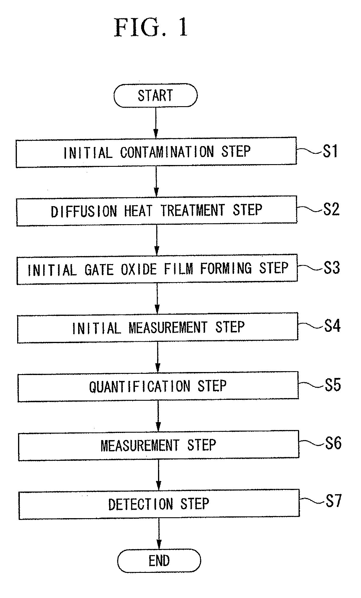
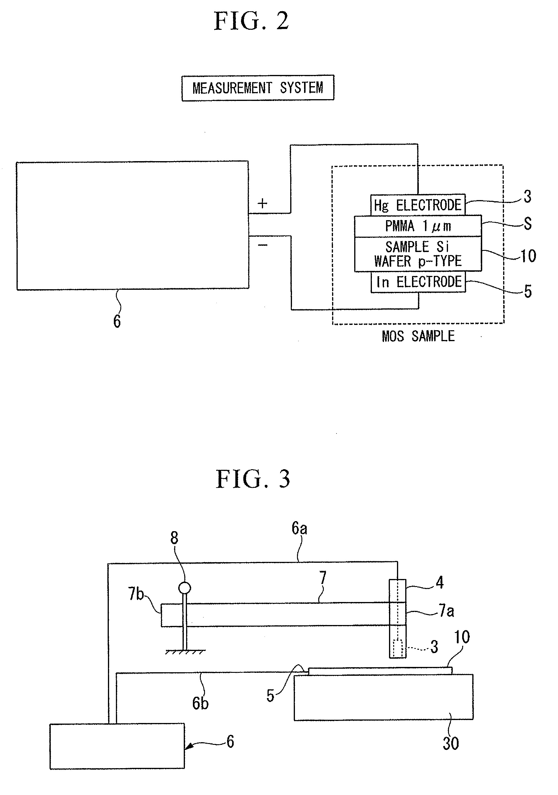
[0034]According to the embodiment, the semiconductor substrate (a semiconductor chip and a silicon wafer) that is subjected to measurement and detection of heavy metal contamination, includes a silicon substrate (wafer) whic...


PUM


Abstract

A method of detecting heavy metal in a semiconductor substrate, includes: a gate oxide film forming step of forming an organic oxide film by spin coating or a sol-gel process, and forming a metal/oxide film/semiconductor junction element by using a mercury probe method; and a step of detecting and quantifying heavy metal by calculating the surface concentration of the heavy metal from junction capacitance characteristics of the element.

Description

BACKGROUND OF THE INVENTION[0001]1. Field of the Invention[0002]The present invention relates to a method of detecting heavy metal in a semiconductor substrate, and more particularly, to a technique used for a method of detecting heavy metal in a thin semiconductor chip or a silicon wafer.[0003]Priority is claimed on Japanese Patent Application No. 2008-105782, filed on Apr. 15, 2008, the content of which is incorporated herein by reference.[0004]2. Description of the Related Art[0005]With the development of mobile phones, small and light electronic components are required to be mounted inside the devices. Accordingly, in order to reduce the thickness of a semiconductor package, a thinning process is performed to make the thickness of a semiconductor chip to be as small as possible. In the thinning process, a gettering sink for gettering heavy metal when heavy metal contamination occurs is thinned by the thinning process. Therefore, a gettering capability is significantly degraded, ...

Claims


Application Information

Patent Timeline
IPC IPC(8): H01L21/66
CPCH01L22/14H01L2924/0002H01L2924/00
Inventor KURITA, KAZUNARI
Owner SUMCO CORP
Why Eureka
Try Eureka