Method for forming quantum well structure and method for manufacturing semiconductor light emitting element

a technology of light emitting elements and well structures, which is applied in the direction of semiconductor devices, electrical equipment, and nanotechnology, etc., can solve the problems of difficult suppression of insufficient composition at an early growth stage of well layers, and inability to suppress light emission wavelength spread, etc., to reduce the variation in composition in the thickness direction of well layers.

Active Publication Date: 2009-10-15
SUMITOMO ELECTRIC IND LTD
View PDF15 Cites 22 Cited by
  • Summary
  • Abstract
  • Description
  • Claims
  • Application Information

AI Technical Summary

Benefits of technology

[0019]According to the method for forming a quantum well structure and method for manufacturing a semiconductor light emitting element of the present invention, the variation in the In composition in the thickness direction of the well layer can be reduced.

Problems solved by technology

However, through research carried out by the inventors of the present invention, it was found that, due to the difference in lattice constant between the barrier layer and the well layer, the In composition is insufficient at an early growth stage of the well layer.
Accordingly, the variation in the In composition unfavorably occurs in the thickness direction of the well layer, and as a result, it becomes difficult to suppress the spread of light emission wavelength.
However, when it is attempted to obtain a higher In composition by decreasing the growth temperature of the well layer lower than that of the barrier layer, the above problem caused by the variation in the In composition in the thickness direction becomes apparent.

Method used


Image

  • Method for forming quantum well structure and method for manufacturing semiconductor light emitting element
  • Method for forming quantum well structure and method for manufacturing semiconductor light emitting element
  • Method for forming quantum well structure and method for manufacturing semiconductor light emitting element

Examples


example

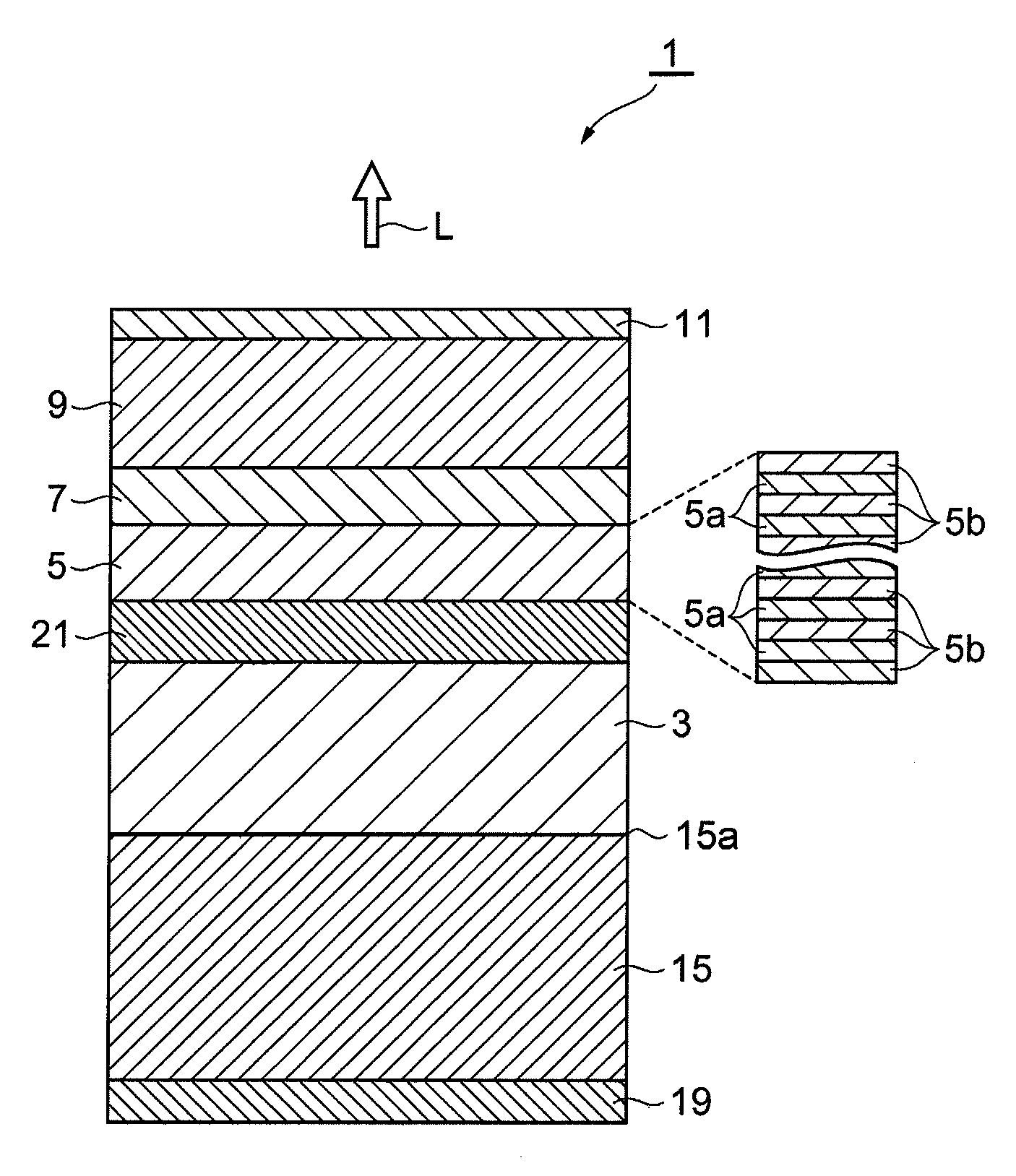
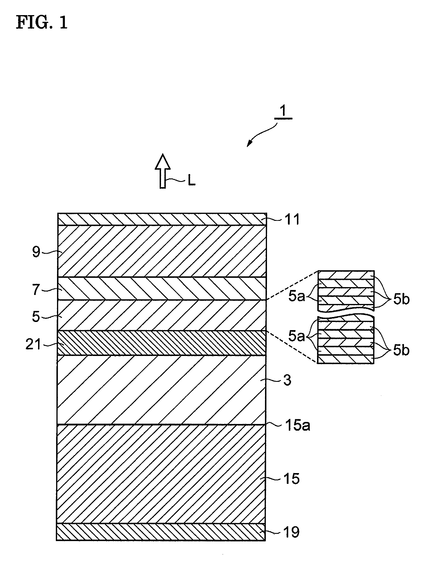
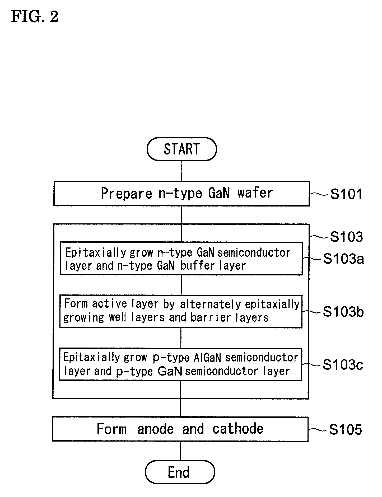
[0068]Next, one example of a method for manufacturing a green light emitting diode structure including high In composition well layers will be described.

[0069]First, after a GaN substrate (corresponding to the n-type GaN substrate 40 shown in FIG. 3A) having a primary surface inclined in an a-axis direction by 18° with respect to the c-plane was placed in a reaction furnace, while the pressure inside the reaction furnace was maintained at 27 kPa and a NH3 gas and a H2 gas were supplied thereto, a heat treatment was performed for 10 minutes at a temperature of 1,050° C. Subsequently, the substrate temperature in the reaction furnace was set to 1,150° C., and by supplying monomethylsilane (MMSi) functioning as an n-type doping source together with TMG and NH3, an n-type GaN layer (corresponding to the n-type GaN semiconductor layer 41 shown in FIG. 3B) was grown so as to have a thickness of 2 μm.

[0070]Subsequently, the substrate temperature was decreased to 800° C., and by supplying T...


PUM


Abstract

A method for forming a quantum well structure that can reduce the variation in the In composition in the thickness direction of a well layer and a method for manufacturing a semiconductor light emitting element are provided. In a step of forming a quantum well structure (active layer) by alternately growing barrier layers and well layers on a primary surface of a GaN substrate, the well layers are each formed by growing InGaN, the barrier layers are each grown at a first temperature, the well layers are each grown at a second temperature which is lower than that of the first temperature, and when the well layers are each formed, before a starting material gas for Ga (trimethylgallium) is supplied, a starting material gas for In is supplied.

Description

BACKGROUND OF THE INVENTION[0001]1. Field of the Invention[0002]The present invention relates to a method for forming a quantum well structure and a method for manufacturing a semiconductor light emitting element.[0003]2. Description of the Related Art[0004]In recent years, some type of group III nitride-based semiconductor light emitting element includes an active layer having a multiquantum well (MQW) structure in which well layers each composed of a group III nitride semiconductor which includes indium (hereinafter referred as “In” in some cases) and another group III element (such as gallium) and barrier layers each composed of GaN or InGaN which has a band gap wider than that of each well layer are alternately laminated to each other. In the MQW structure as described above, when the well layer is grown on the barrier layer, a starting material gas for In (such as trimethylindium), a starting material gas for the other group III element (such as trimethylgallium), and a startin...

Claims


Application Information

Patent Timeline
Patent Type & Authority Applications(United States)
IPC IPC(8): H01L33/00H01L21/20B82Y10/00B82Y20/00B82Y40/00H01L21/205H01L33/04H01L33/06H01L33/32
CPCH01L21/02389H01L21/02433H01L21/02458H01L33/06H01L21/0262H01L33/0075H01L21/0254
Inventor ENYA, YOHEIYOSHIZUMI, YUSUKEUENO, MASAKINAKANISHI, FUMITAKE
Owner SUMITOMO ELECTRIC IND LTD
Why Eureka
Try Eureka