Carrier substrate and method of manufacturing flexible display apparatus using the same

a technology of carrier substrate and flexible display, which is applied in the direction of record information storage, catalyst activation/preparation, synthetic resin layered products, etc., can solve the problems of adhesive material, application and use limit, etc., and achieve the effect of reducing a manufacturing cos

Inactive Publication Date: 2009-10-22
SAMSUNG DISPLAY CO LTD
View PDF18 Cites 48 Cited by
  • Summary
  • Abstract
  • Description
  • Claims
  • Application Information

AI Technical Summary

Benefits of technology

[0027]According to the above, the carrier substrate including the sacrificial layer and the adhesive layer may be recycled, thereby reducing a manufacturing cost.

Problems solved by technology

However, since the conventional LCD, PDP, and OLED employ a glass substrate having no flexibility, they have a limitation in applications and the use thereof.
However, since the substrate of a flexible display apparatus has flexibility, many problems may occur when manufacturing a TOP panel by directly introducing the plastic substrate into the manufacturing process of a conventional glass substrate.
However, when adopting the above method, many difficulties exist in development of an adhesive material that endures a high-temperature process and enables the carrier substrate to be easily separated from the plastic substrate after forming the array of the thin film transistors.

Method used


Image

  • Carrier substrate and method of manufacturing flexible display apparatus using the same
  • Carrier substrate and method of manufacturing flexible display apparatus using the same
  • Carrier substrate and method of manufacturing flexible display apparatus using the same

Examples


first embodiment

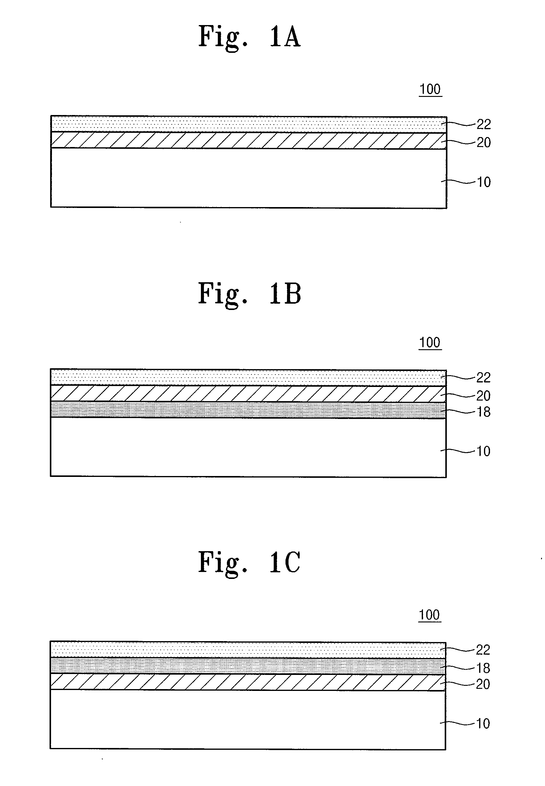
[0039]FIG. 1A is a sectional view showing a carrier substrate 100 according to the present invention.

[0040]As shown in FIG. 1A, the carrier substrate 100 according to the first embodiment of the present invention includes a rigid substrate 10, an adhesive layer 22, and a sacrificial layer 20. The adhesive layer 22 is formed above the rigid substrate 10 and has an adhesive property. The sacrificial layer 20 is interposed between the rigid substrate 10 and the adhesive layer 22. The sacrificial layer 20 includes a material selected from the group consisting of a transparent metal oxide, an alkaline water-soluble polymer compound, and an acid water-soluble polymer compound.

[0041]The rigid substrate 10 may include a material allowing a laser beam to pass therethrough. For example, the rigid substrate 10 may include at least one selected from the group consisting of E2K, borosilicate glass, fused silica glass, sapphire, and quartz.

[0042]The sacrificial layer 20 may include a material sel...

second embodiment

[0049]FIG. 1B is a sectional view showing a carrier substrate 100 according to the present invention.

[0050]As shown in FIG. 1B, the carrier substrate 100 according to the second embodiment of the present invention includes a rigid substrate 10, an adhesive layer 22, and a sacrificial layer 20, and further includes an etching promoter 18 provided under the sacrificial layer 20. The adhesive layer 22 is formed on the rigid substrate 10 and has an adhesive property. The sacrificial layer 20 is interposed between the rigid substrate 10 and the adhesive layer 22. The sacrificial layer 20 includes a material selected from the group consisting of a transparent metal oxide, an alkaline water-soluble polymer compound, and an acid water-soluble polymer compound. For the purpose of explanation, the same reference numerals will be assigned to the elements identical to those of the previous embodiment, and detailed description thereof will be omitted in order to avoid redundancy.

[0051]The etchin...

third embodiment

[0056]Although the etching promoter 18 is formed under the sacrificial layer 20 according to the present embodiment, the present invention is not limited thereto. For example, the etching promoter 18 may be formed on the sacrificial layer 20 as shown in FIG. 1C illustrating a carrier substrate 100 according to the present invention.

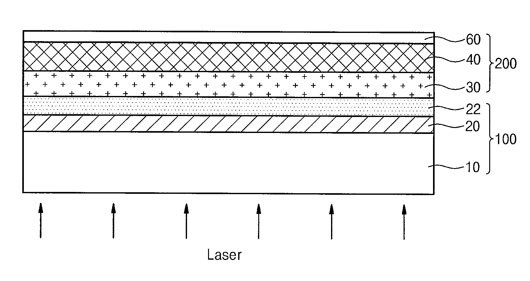
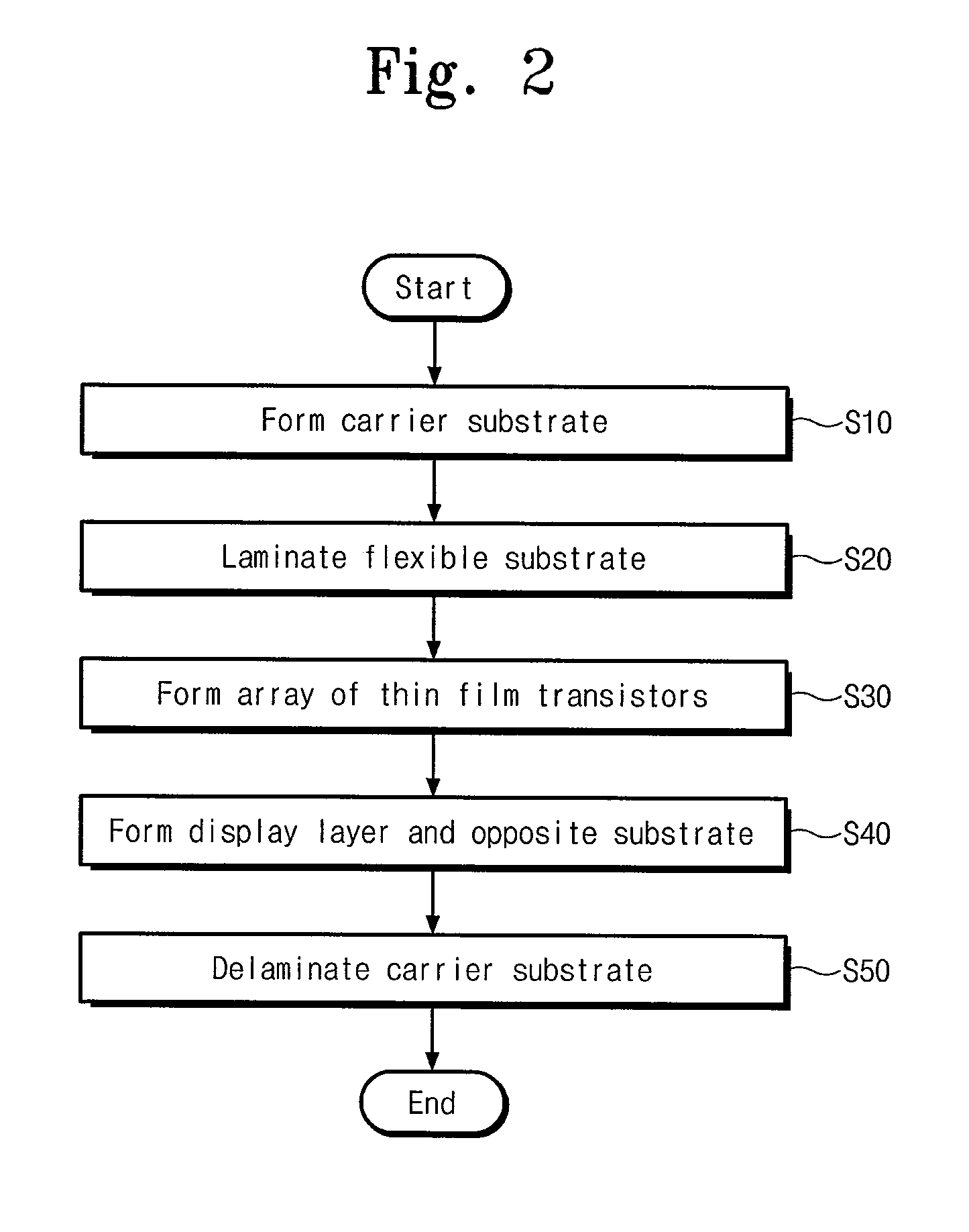
[0057]FIG. 2 is a flowchart illustrating the method of manufacturing the flexible display apparatus using the carrier substrate 100 according to an exemplary embodiment of the present invention, and FIGS. 3A to 3H are sectional views showing a method of manufacturing an electrophoresis display apparatus as the method of manufacturing the flexible display apparatus according to the first embodiment of the present invention.

[0058]Referring to FIG. 2, in the method of manufacturing the flexible display apparatus using the carrier substrate 100 according to an exemplary embodiment of the present invention, the carrier substrate 100 is formed (S10), a flexible...


PUM

PropertyMeasurementUnit
thicknessaaaaaaaaaa
thicknessaaaaaaaaaa
sizeaaaaaaaaaa

Abstract

Disclosed are a carrier substrate which can be recycled and a method of manufacturing a flexible display apparatus using the same. The carrier substrate includes a rigid substrate, an adhesive layer, and a sacrificial layer. The adhesive layer is formed on the rigid substrate and has an adhesive property. The sacrificial layer is interposed between the rigid substrate and the adhesive layer. The sacrificial layer includes a material selected from the group consisting of a transparent metal oxide, an alkaline water-soluble polymer compound, and an acid water-soluble polymer compound.

Description

CROSS-REFERENCE TO RELATED APPLICATION[0001]This application claims priority to Korean Patent Application No. 2008-35700 filed on Apr. 17, 2008, the contents of which are herein incorporated by reference in their entirety.BACKGROUND[0002]1. Field of the Invention[0003]The present invention relates to a carrier substrate used to manufacture a flexible display apparatus and a method of manufacturing a flexible display apparatus using the same.[0004]2. Description of the Related Art[0005]As information technologies are developed the demand for high-performance display apparatuses capable of displaying various types of information, such as videos, graphics, and characters to achieve high-speed transmission of the information has increased. According to such demands, the display industry has grown rapidly. Recently, flat panel displays (FPD) have been spotlighted because the FPDs can be fabricated in a large size with a slim and light structure.[0006]Such an FPD includes a liquid crystal...

Claims


Application Information

Patent Timeline
Patent Type & Authority Applications(United States)
IPC IPC(8): C23F1/00B32B33/00B32B5/00B32B5/18B32B38/10
CPCB32B7/12B32B37/12B32B38/10B32B2310/0843Y10T428/265G02F1/133305G02F2202/28Y10T428/2848B32B2457/20B32B7/06B32B9/002B32B9/045B32B27/08B32B27/281B32B27/285B32B27/286B32B27/36B32B2255/00B32B2255/20B32B2255/26B32B2255/28B32B2307/546B32B2307/726B32B2307/748Y10T428/249983G02F1/13B01J37/02
Inventor KIM, MYUNG-HWAN
Owner SAMSUNG DISPLAY CO LTD
Why Eureka
Try Eureka