Voltage generating circuit and semiconductor device having the same

a voltage generator and circuit technology, applied in the field of voltage generators, can solve the problems of increasing power consumption of psram, affecting the reliability of active mode voltage generators, and operating unstably, so as to reduce power consumption, reduce body effects, and improve the reliability of active elements implementing

Active Publication Date: 2009-10-22
SAMSUNG ELECTRONICS CO LTD
View PDF6 Cites 4 Cited by
  • Summary
  • Abstract
  • Description
  • Claims
  • Application Information

AI Technical Summary

Benefits of technology

[0016]Consequently, the voltage generating circuit according to example embodiments may not only improve reliability of the active elements implementing the circuit but also reduce the power consumption. Moreover, the voltage generating circuit including the active charge pumping circuit may stably generate the active voltage which is higher than the power supply voltage by reducing the body effect.

Problems solved by technology

However, the data cells in the PSRAM may be periodically refreshed to prevent or reduce a data retention failure in a standby mode, and thus, the PSRAM may increase power consumption.
Circuit elements included in a voltage generator for generating the voltage for the active mode may be damaged by high operation voltages and also operate unstably due to a variance of a threshold voltage caused by a body effect.

Method used


Image

  • Voltage generating circuit and semiconductor device having the same
  • Voltage generating circuit and semiconductor device having the same
  • Voltage generating circuit and semiconductor device having the same

Examples


Embodiment Construction

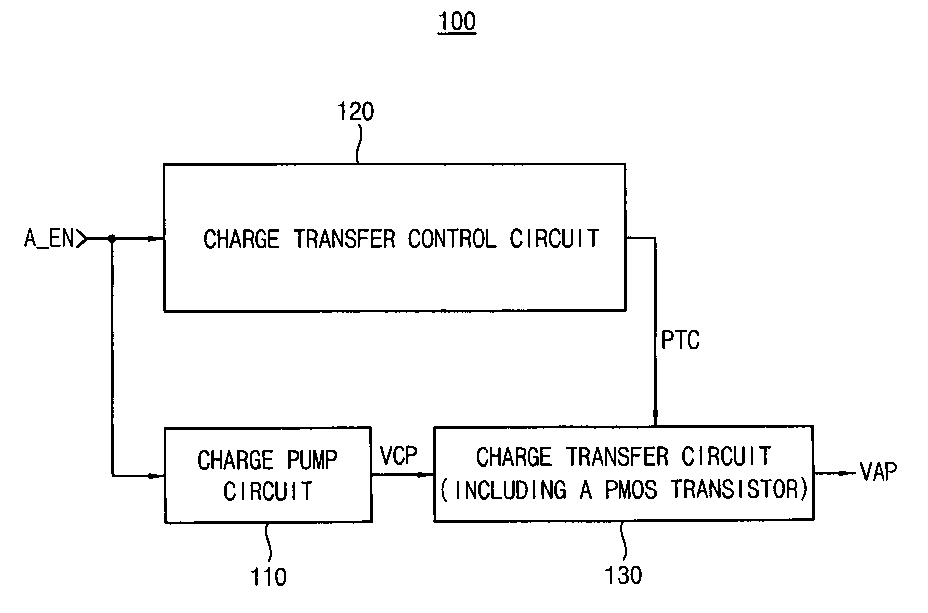
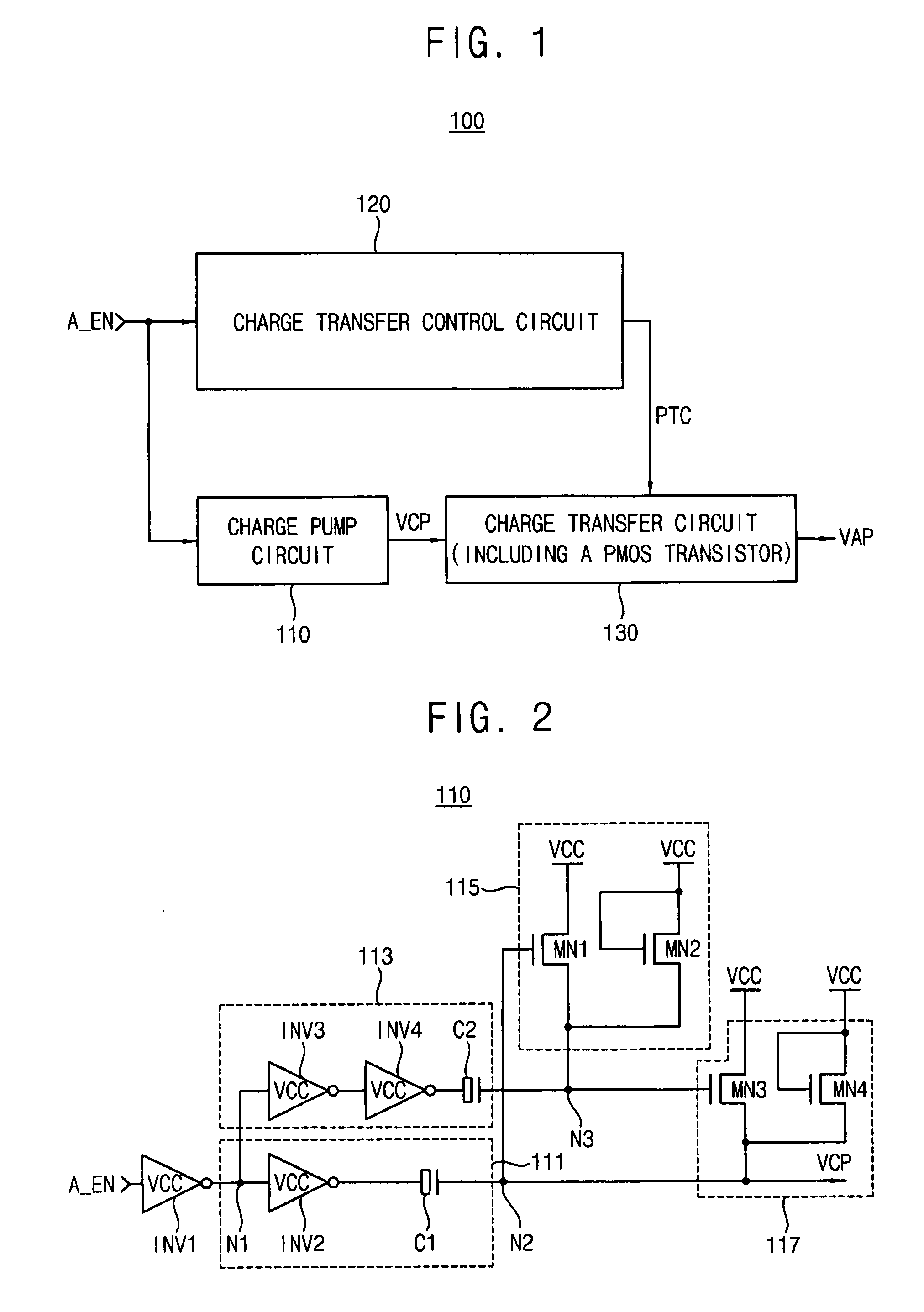
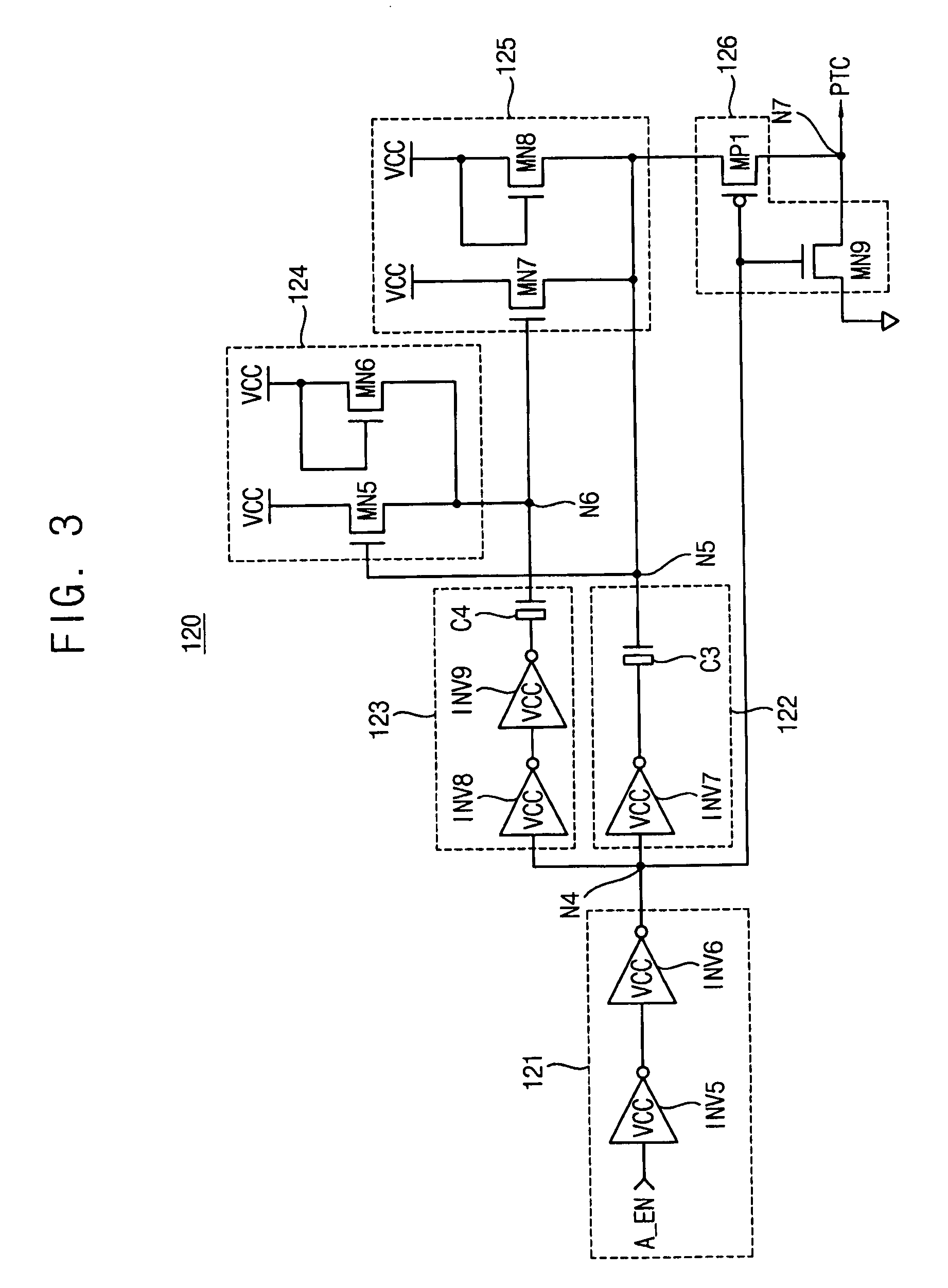
[0028]Example embodiments now will be described more fully with reference to the accompanying drawings, in which example embodiments are shown. Example embodiments may, however, be embodied in many different forms and should not be construed as limited to example embodiments set forth herein. Rather, these embodiments are provided so that this disclosure will be thorough and complete, and will fully convey the scope of example embodiments to those skilled in the art. Like reference numerals refer to like elements throughout this application.

[0029]It will be understood that, although the terms first, second, etc. may be used herein to describe various elements, these elements should not be limited by these terms. These terms are used to distinguish one element from another. For example, a first element could be termed a second element, and, similarly, a second element could be termed a first element, without departing from the scope of example embodiments. As used herein, the term “a...


PUM


Abstract

An active charge pump circuit may include a charge pump circuit, a control circuit, and a charge transfer circuit. The charge pump circuit may generate a charge pumping voltage in response to an active enable signal. The control circuit may generate a charge transfer control signal varying between a ground voltage and a boosted power supply voltage that is twice as much as a power supply voltage in response to the active enable signal. The charge transfer circuit may output the charge pumping voltage as an active voltage in response to the charge transfer control signal.

Description

PRIORITY STATEMENT[0001]This application claims priority under 35 USC §119 to Korean Patent Application No. 2008-0036119, filed on Apr. 18, 2008 in the Korean Intellectual Property Office (KIPO), the entire contents of which are incorporated herein by reference.BACKGROUND[0002]1. Technical Field[0003]Example embodiments relate to a voltage generator, and more particularly, to a voltage generator including an active charge pump circuit and a semiconductor device including the voltage generator.[0004]2. Description of the Related Art[0005]Recently, as a system on a chip (SOC) is developed, the memory devices included in the SOC need to be faster, lighter, and smaller. Therefore, a pseudo static random access memory (PSRAM) is generally used in the SOC. The PSRAM is implemented by embedded dynamic random access memory (eDRAM). A structure of PSRAM is substantially the same as a structure of a DRAM but the PSRAM operates as a SRAM as seen from an exterior. The PSRAM has the high density...

Claims


Application Information

Patent Timeline
Patent Type & Authority Applications(United States)
IPC IPC(8): G05F1/10
CPCG11C5/145H02M3/07G11C11/4074
Inventor JOO, JONG-DOO
Owner SAMSUNG ELECTRONICS CO LTD
Why Eureka
Try Eureka