Nitride-based semiconductor device and method of manufacturing the same

a technology of nitride and semiconductors, applied in semiconductor lasers, solid-state devices, lasers, etc., can solve the problems of excessive heat generation in the device, disadvantageous reduction of the luminous efficiency of the light-emitting device, and likely defects on the semiconductor layer, etc., to achieve easy division and small thickness

Active Publication Date: 2009-10-29
EPISTAR CORP
View PDF6 Cites 268 Cited by
  • Summary
  • Abstract
  • Description
  • Claims
  • Application Information

AI Technical Summary

Benefits of technology

[0036]In other words, in the aforementioned method of manufacturing a nitride-based semiconductor device according to the third aspect, the step of separating into chips preferably includes a step of separating into chips so as to divide the nitride-based semiconductor layers into the individual the semiconductor light-emitting devices on the bottom portions of the recess portions of the regions where the first side surfaces and the second side surfaces are opposed to each other. According to this structure, a thickness of substrate on the bottom portions of the recess portions are smaller than that of the substrate other than the bottom portions of the recess portions, and hence the wafer can be easily divided on the portions, having smaller thickness, of the substrate.
[0037]In the aforementioned method of manufacturing a nitride-based semiconductor device according to the third aspect, the step of growing the nitride-based semiconductor layers preferably includes a step of growing the nitride-based semiconductor layers so that the plane area of the nitride-based semiconductor layers is reduced in a direction away from the substrate along a thickness direction of the nitride-based semiconductor layers by the first side surfaces and the second side surfaces. According to this structure, larger spaces (regions where the first side surfaces and the second side surfaces are opposed to each other in a wafer state (upper regions of the step portions)) than a plane area of the recess portions of the substrate is formed on the surface of the semiconductor layer on a side opposite to the substrate by the first side surfaces and the second side surfaces, and hence the wafer can be easily divided between the first side surfaces and the second side surfaces when separating the semiconductor device into chips.
[0038]In the aforementioned method of manufacturing a nitride-based semiconductor device according to the third aspect, the nitride-based semiconductor device preferably comprises light-emitting layers having optical waveguides, and the step of growing the nitride-based semiconductor layers includes a step of growing the nitride-based semiconductor layers so that the first side surfaces and the second side surfaces extend along an extensional direction of the optical waveguides. According to this structure, the first and

Problems solved by technology

In a manufacturing process for the semiconductor chip disclosed in each of the aforementioned Japanese Patent No. 2780618 and Japanese Patent Laying-Open No. 11-224866, however, defects are likely to be caused on the semiconductor layer when forming the dividing grooves because they are formed by etching, mechanically scribing or laser scribing the semiconductor layer which is formed on the substrate by crystal growth.
In a case where the nitride-based semiconductor device is the light-emitting device, when the defects reach an emission layer constituting the semiconducto

Method used


Image

  • Nitride-based semiconductor device and method of manufacturing the same
  • Nitride-based semiconductor device and method of manufacturing the same
  • Nitride-based semiconductor device and method of manufacturing the same

Examples


first embodiment

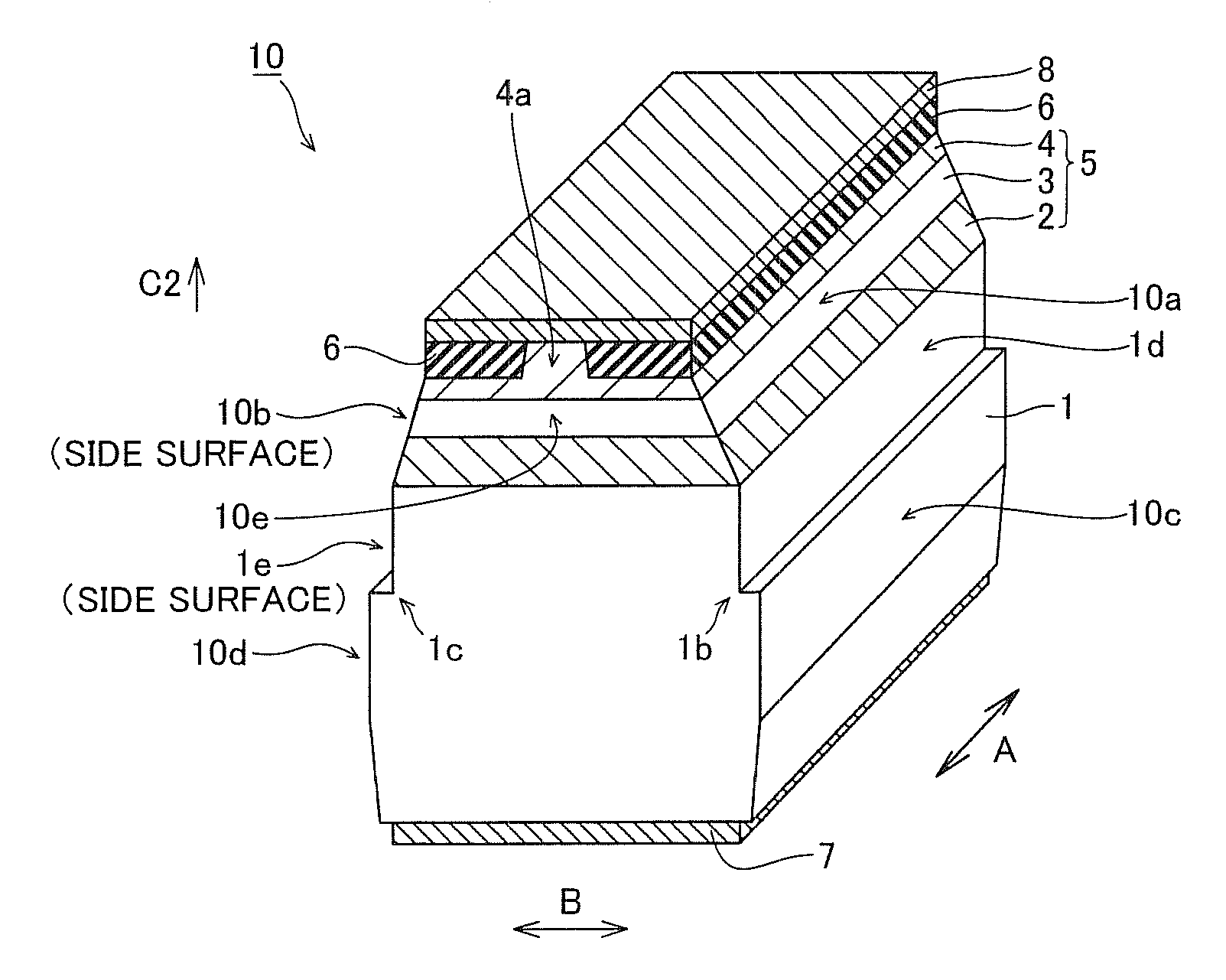
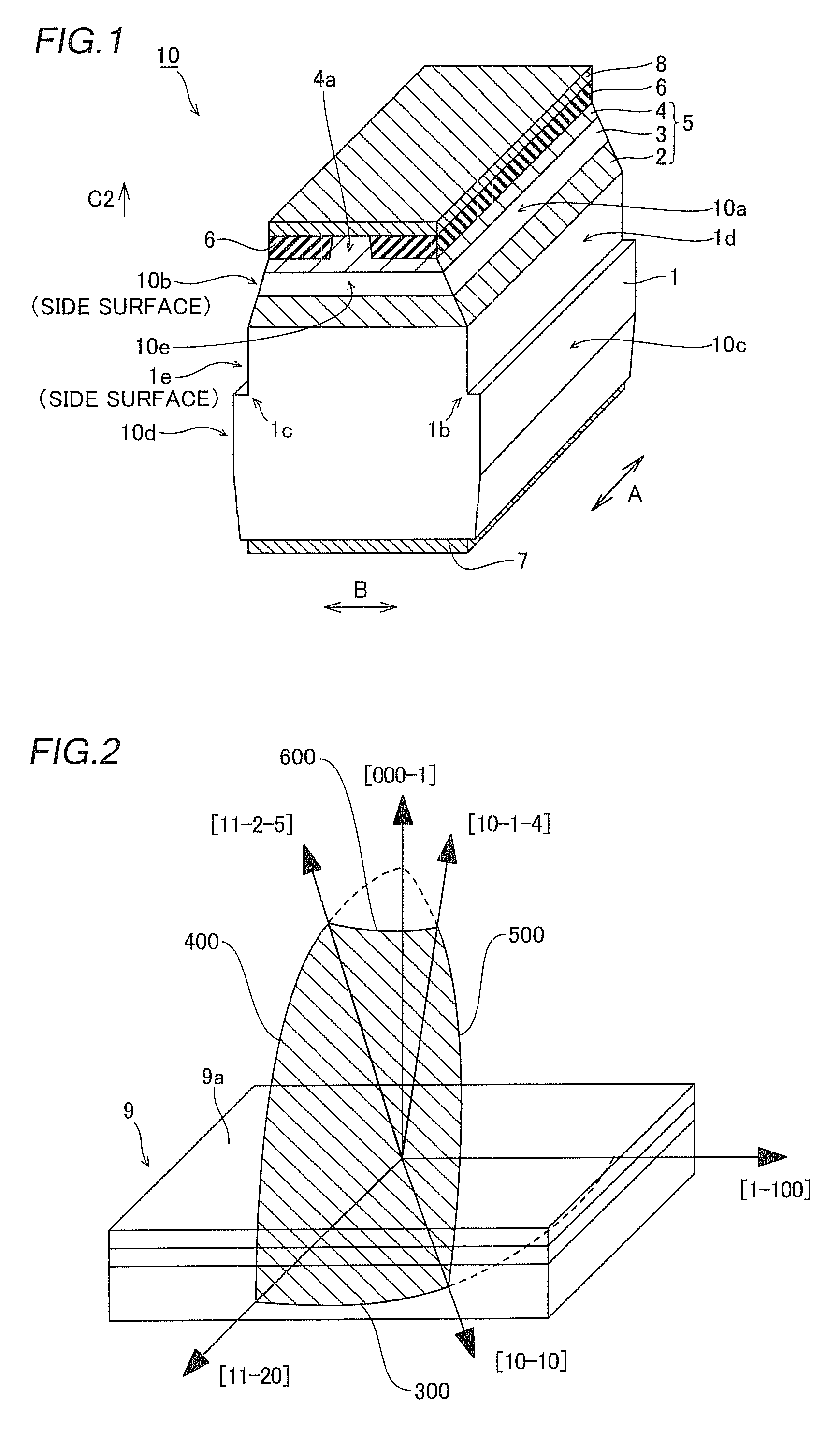
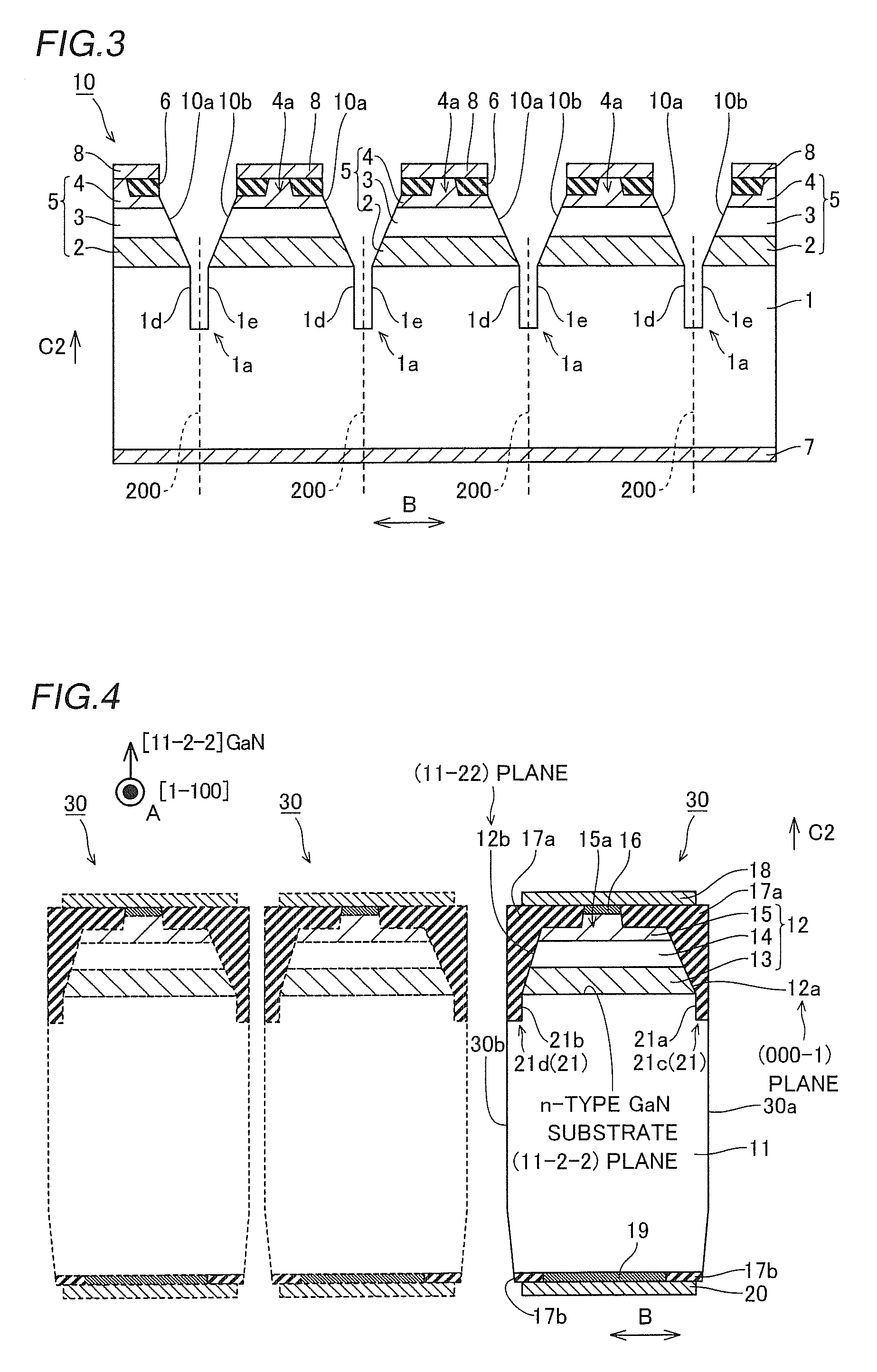
[0088]A structure of a nitride-based semiconductor laser device 30 according to a first embodiment will be described with reference to FIGS. 4 and 5.

[0089]This nitride-based semiconductor laser device 30 according to the first embodiment is formed by a wurtzite nitride semiconductor whose a main surface is a (11-2-2) plane.

[0090]In the nitride-based semiconductor laser device 30, a light-emitting device layer 12 is formed on an n-type GaN substrate 11 having a thickness of about 100 μm, as shown in FIG. 4. The light-emitting device layer 12 is formed with an n-type cladding layer 13 made of n-type Al0.05Ga0.95N, having a thickness of about 2.0 μm and an emission layer 14 having an MQW structure in which a well layer (not shown) made of Ga0.7In0.3N having a thickness of about 3 nm and a barrier layer (not shown) made of GaN having a thickness of about 20 nm are stacked. A p-type cladding layer 15 made of p-type Al0.05Ga0.5N, having a thickness of about 0.5 μm and including a projecti...

second embodiment

[0115]A light-emitting device layer 42 is formed after forming an underlayer 50 made of AlGaN on an n-type GaN substrate 11 in a second embodiment dissimilarly to the aforementioned first embodiment, which will be hereinafter described with reference to FIG. 11.

[0116]A nitride-based semiconductor laser device 40 according to the second embodiment is formed by a wurtzite nitride-based semiconductor whose main surface is a (11-2-2) plane.

[0117]In the nitride-based semiconductor laser device 40, the emission layer 42 is formed on the n-type GaN substrate 11 having a thickness of about 100 μm through the underlayer 50 made of Al0.05Ga0.95N having a thickness of about 3 to 4 μm, as shown in FIG. 11. On this underlayer 50, a plurality of groove-shaped cracks 51 are so formed as to extend in a cavity direction (direction perpendicular to the plane of FIG. 11). The cracks 51 are examples of the “recess portion” in the present invention. The n-type GaN substrate 11 according to the second em...

third embodiment

[0128]In a manufacturing process for a nitride-based semiconductor laser device 60 according to a third embodiment, positions of forming cracks 71 are controlled by forming scribed grooves 70 of dashed line shapes on an underlayer 50 on an n-type GaN substrate 61 dissimilarly to the aforementioned second embodiment, which will be hereinafter described with reference to FIGS. 12 and 14 to 16. The n-type GaN substrate 61 is an example of the “base substrate” in the present invention, and the cracks 71 are examples of the “recess portion” in the present invention.

[0129]This nitride-based semiconductor laser device 60 according to the third embodiment is formed by a wurtzite nitride-based semiconductor whose main surface is a (1-10-2) plane.

[0130]The remaining structure of the nitride-based semiconductor laser device 60 according to the third embodiment is similar to that of the aforementioned second embodiment.

[0131]In a manufacturing process for the nitride-based semiconductor laser d...


PUM


Abstract

A nitride-based semiconductor device includes a substrate, a first step portion formed on a main surface side of a first side end surface of the substrate, a second step portion formed on the main surface side of a second side end surface substantially parallel to the first side end surface on an opposite side of the first side end surface and a nitride-based semiconductor layer whose first side surface is a (000-1) plane starting from a first side wall of the first step portion and a second side surface starting from a second side wall of the second step portion on the main surface.

Description

CROSS-REFERENCE TO RELATED APPLICATIONS [0001]The priority application numbers JP2008-115373, Nitride-Based Semiconductor Light-Emitting Device and Method of Manufacturing the Same, Apr. 25, 2008, Yasuto Miyake et al, JP2009-76259, Nitride-Based Semiconductor Light-Emitting Device and Method of Manufacturing the Same, Mar. 26, 2009, Yasuto Miyake et al, upon which this patent application is based are hereby incorporated by reference.BACKGROUND OF THE INVENTION[0002]1. Field of the Invention[0003]The present invention relates to a nitride-based semiconductor device and a method of manufacturing the same.[0004]2. Description of the Background Art[0005]In general, a light-emitting device made of a nitride-based material such as gallium nitride (GaN) has been put into practice as a 405 nm blue-violet semiconductor laser (LD) as a light source for recording / playback employed as a DVD system. A semiconductor laser device emitting blue or green light, employing a nitride-based material has...

Claims


Application Information

Patent Timeline
IPC IPC(8): H01L29/06H01L33/00H01L21/78H01L21/338H01L29/778H01L29/812H01L33/06H01L33/32H01L33/42H01S5/343
CPCB82Y20/00H01S2304/12H01L21/02433H01L21/0254H01L29/2003H01L29/812H01L33/20H01L33/32H01S5/0201H01S5/02212H01S5/02272H01S5/02276H01S5/0425H01S5/22H01S5/2201H01S5/2214H01S5/3202H01S5/34333H01L21/0242H01L2224/32145H01L2224/48247H01L2224/48465H01L2224/48471H01L2224/73265H01L2224/45144H01S5/32025H01S2301/176H01S5/0237H01S5/02345H01L2924/00
Inventor MIYAKE, YASUTOHIROYAMA, RYOJIHATA, MASAYUKIKUNO, YASUMITSU
Owner EPISTAR CORP
Why Eureka
Try Eureka