Method for forming carbon silicon alloy (CSA) and structures thereof

a technology of carbon silicon alloy and epitaxial growth, which is applied in the direction of basic electric elements, electrical equipment, semiconductor devices, etc., can solve the problems of limiting the use of such epitaxial chemistries of si precursors and etchants for selective deposition of csa, complicated epitaxial growth of csa layers, and compromising the effectiveness of typical etchants, etc., to achieve the effect of enhancing deposition/growth rate, enhancing substitutionality and substitution ra

Inactive Publication Date: 2009-10-29
IBM CORP
View PDF12 Cites 27 Cited by
  • Summary
  • Abstract
  • Description
  • Claims
  • Application Information

AI Technical Summary

Benefits of technology

[0008]Methods for forming carbon silicon alloy (CSA) and structures thereof are disclosed. The method provides improvement in substitutionality and deposition rate of carbon in epitaxially grown carbon silicon alloy layers (i.e., substituted carbon in Si lattice). In one embodiment of the disclosed method, a carbon silicon alloy layer is epitaxially grown on a substrate at an intermediate temperature with a silicon precursor, a carbon (C) precursor in the presence of an etchant and a trace amount of germanium material (e.g., germane (GeH4)). The intermediate temperature increases the percentage of substitutional carbon in epitaxially grown CSA layer and avoids any tendency for silicon carbide to form. The presence of the trace amount of germanium material, of approximately less than 1% to approximately 5%, in the resulting epitaxial layer, has an effect of stabilizing and enhancing deposition / growth rate without compromising the tensile stress of CSA layer formed thereby.

Problems solved by technology

However, epitaxial growth of CSA layers is very complicated for a number of reasons.
Another challenge in the epitaxial growth of CSA layers may include the low solid solubility of carbon (C) in a Si lattice.
However, the low temperature may compromise the effectiveness of a typical etchant (e.g., hydrogen chloride (HCl)) for promoting selective epitaxial growth of CSA.
This result limits the use of such epitaxial chemistries of Si precursors and etchants for selective deposition of CSA.

Method used


Image

  • Method for forming carbon silicon alloy (CSA) and structures thereof
  • Method for forming carbon silicon alloy (CSA) and structures thereof
  • Method for forming carbon silicon alloy (CSA) and structures thereof

Examples


Embodiment Construction

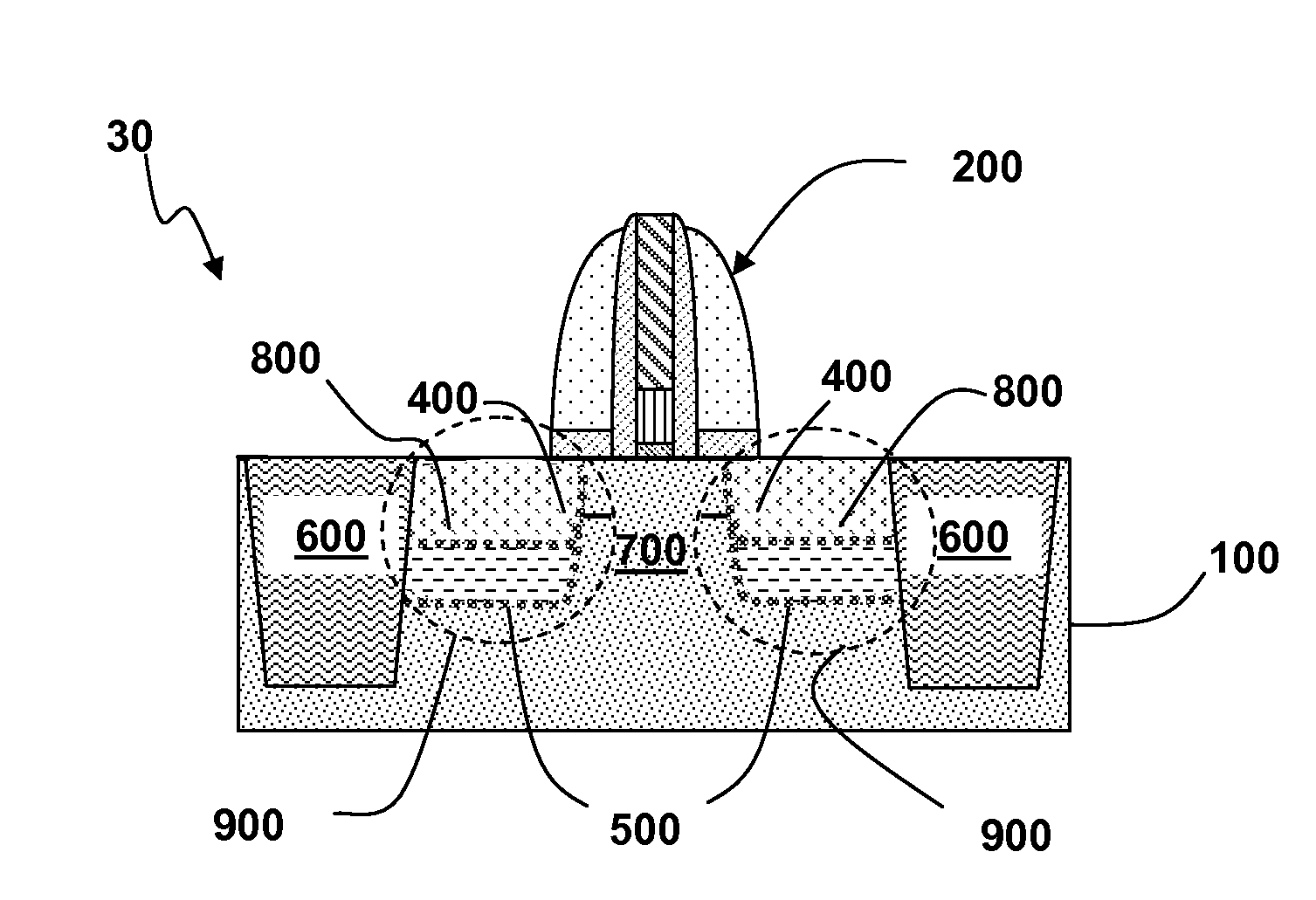
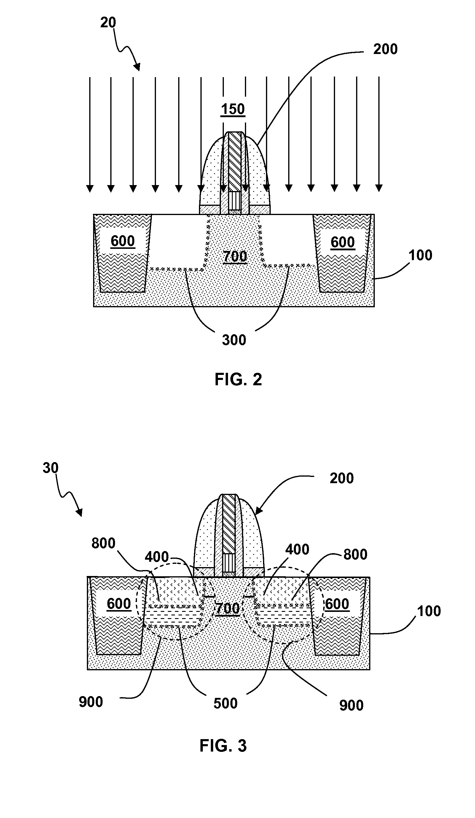
[0022]Embodiments depicted in the drawings in FIG. 1-3 illustrate the methods and various resulting structure(s) of the different aspects of fabricating an nFET 30 (FIG. 3) in a CMOS using epitaxial layers of CSA disposed on a substrate 100 (FIGS. 2 and 3). Examples of tests results of performance of structures formed by the disclosed method are illustrated in FIGS. 4A-5A.

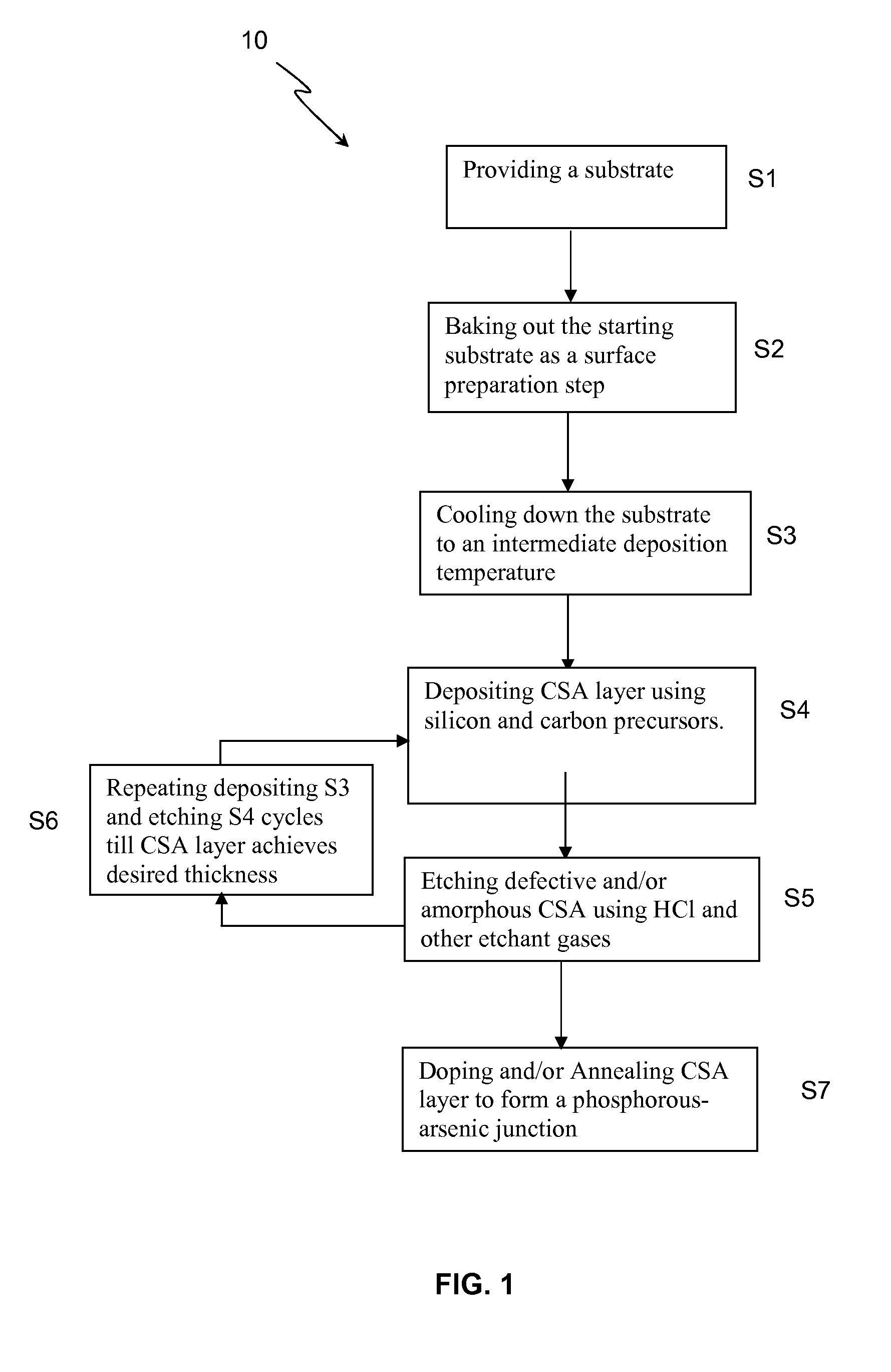
[0023]FIG. 1 illustrates a flow diagram of a process including processes S1-S7 of an embodiment of the disclosed method. A CMOS semiconductor structure 20 as shown in FIG. 2 is provided in process S1. Semiconductor structure 20 is fabricated according to currently known or later developed techniques. The structure 20 may include a gate 200 disposed on a substrate 100. Substrate 100 may include silicon sites, for example, recesses 300 shown in FIG. 2 and non-silicon sites, for example, shallow trench isolation (STI) 600, incorporated therein. Recesses 300 are formed using currently known or later developed etching t...


PUM

PropertyMeasurementUnit
temperatureaaaaaaaaaa

Abstract

Methods for forming carbon silicon alloy (CSA) and structures thereof are disclosed. The method provides improvement in substitutionality and deposition rate of carbon in epitaxially grown carbon silicon alloy layers (i.e., substituted carbon in Si lattice). In one embodiment of the disclosed method, a carbon silicon alloy layer is epitaxially grown on a substrate at an intermediate temperature with a silicon precursor, a carbon (C) precursor in the presence of an etchant and a trace amount of germanium material (e.g., germane (GeH4)). The intermediate temperature increases the percentage of substitutional carbon in epitaxially grown CSA layer and avoids any tendency for silicon carbide to form. The presence of the trace amount of germanium material, of approximately less than 1% to approximately 5%, in the resulting epitaxial layer, has an effect of stabilizing and enhancing deposition / growth rate without compromising the tensile stress of CSA layer formed thereby.

Description

BACKGROUND[0001]1. Technical Field[0002]The disclosure relates generally to formation of carbon silicon alloy (CSA) epitaxial layers during fabrication of N-doped field effect transistors (nFET), and more particularly, to methods of forming CSA epitaxial layers with high degree of substitutional carbon at accelerated growth rates.[0003]2. Background Art[0004]In the current state of the art, epitaxial growth of carbon silicon alloy (CSA) on a silicon substrate is accomplished by chemical vapor deposition (CVD) using a mixture of precursors and etchants in a carrier gas. The carbon is added to generate tensile stress in epitaxially grown CSA layers in order to improve the performance of n-doped field effect transistor (nFET) fabricated therefrom.[0005]However, epitaxial growth of CSA layers is very complicated for a number of reasons. For example, the growth of epitaxial layers is heavily dependent on the substrate surface on which the epitaxial layer is grown (i.e., the crystalline p...

Claims


Application Information

Patent Timeline
Patent Type & Authority Applications(United States)
IPC IPC(8): H01L49/00H01L21/20
CPCH01L21/02381H01L21/02529H01L21/02532H01L21/0262H01L29/7848H01L29/165H01L29/66636H01L29/78H01L21/02636
Inventor CHAKRAVARTI, ASHIMA B.DUBE, ABHISHEKLOESING, RAINERSCHEPIS, DOMINIC J.
Owner IBM CORP
Why Eureka
Try Eureka