

Pll circuit
a technology of pll circuit and gate, applied in the direction of pulse manipulation, pulse automatic control, pulse technique, etc., can solve the problems of gate capacity increase, problem of increasing an area, increasing a consumption current of an analog circuit, etc., and achieve the effect of improving phase difference detection
- Summary
- Abstract
- Description
- Claims
- Application Information
AI Technical Summary
Benefits of technology
Problems solved by technology
Method used
Image

Examples
first embodiment
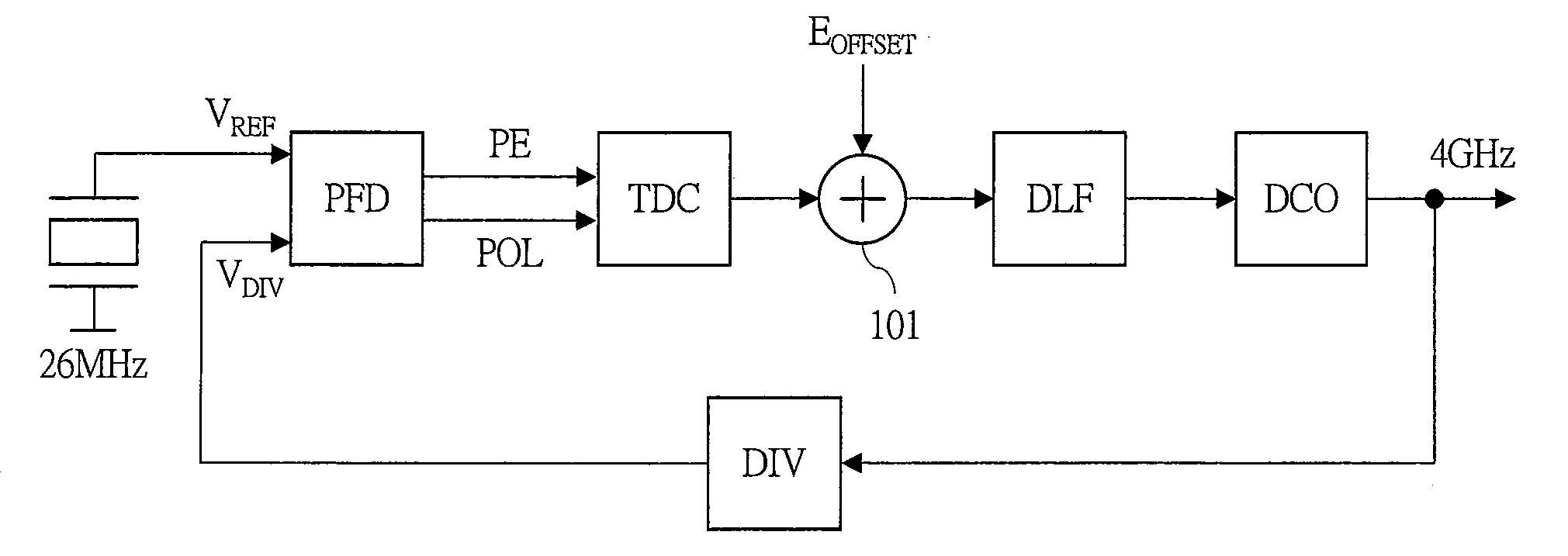
[0077]FIG. 1 is a block diagram showing a configuration example of an ADPLL (all digital phase-locked loop) according to a first embodiment of the present invention.
[0078]First, with reference to FIG. 1, an example of a configuration of the ADPLL according to the first embodiment is explained. The ADPLL according to the first embodiment is, for example, a semiconductor integrated circuit, and is formed over one semiconductor chip by a well-known semiconductor production technique. The ADPLL in FIG. 1 comprises, for example, a phase frequency detector PFD, a time to digital converter TDC, a digital loop filter DLF, a digitally controlled oscillator DCO, a divider DIV and the like.
[0079]The phase frequency detector PFD compares phases and frequencies of a reference signal VREF and a feedback signal VDIV. The time to digital converter TDC converts an output of the phase frequency detector PFD into a digital value. The digital loop filter DLF removes a high frequency noise component fro...
second embodiment
[0092]FIG. 4 is a block diagram showing a configuration example of an ADPLL according to a second embodiment of the present invention.
[0093]First, with reference to FIG. 4, an example of the configuration of the ADPLL according to the second embodiment is explained. The ADPLL according to the second embodiment is, for example, a semiconductor integrated circuit, and is formed over one semiconductor chip by the well-known semiconductor production technique. The ADPLL in FIG. 4 comprises, for example, a phase frequency detector PFD and a time to digital converter TDC (a piece of phase detecting or frequency detecting and time-to-digital converting equipment, hereinafter, referred to as (PFD+TDC)), a digital loop filter DLF, a digitally controlled oscillator DCO, a divider DIV and the like.
[0094]The phase frequency detector PFD compares phases and frequencies of a reference signal VREF and a feedback signal VDIV. The time to digital converter TDC converts an output of the phase frequen...
third embodiment
[0137]In the second embodiment, in the explanations of FIG. 4, FIG. 17 and FIG. 18, an explanation that the phase difference is measured by the counter and remaining factors are measured by the delay-line is made. In a third embodiment, explanations are made from a different viewpoint.
[0138]Since the signal of the VDIV completely synchronizes with the output of the DCO or the output of the divider having an input of the output of the DCO, the phase can be converted into digital in an integral multiple of the output of the DCO or the output of the divider having the input of the output of the DCO. On the other hand, since the VREF does not synchronize with the output of the DCO or the output of the divider having the input of the output of the DCO, the phase cannot be converted into digital in an integral multiple thereof, and accordingly, a certain phase (time) difference occurs. It can be considered that the difference is expressed by the delay-line. That is, operation of this ADPL...
PUM
 Abstract
Description
Claims
Application Information