Complementary metal oxide semiconductor device with an electroplated metal replacement gate

a technology of metal oxide semiconductor and replacement gate, which is applied in the direction of semiconductor devices, basic electric elements, electrical equipment, etc., can solve the problems of increasing the effective gate dielectric thickness and conventional gate structures that are not suitable for future cmos technology generations, so as to enhance plating and enhance electron flow. , the effect of preventing electron flow

Inactive Publication Date: 2009-11-05
GLOBALFOUNDRIES INC
View PDF5 Cites 40 Cited by
  • Summary
  • Abstract
  • Description
  • Claims
  • Application Information

AI Technical Summary

Benefits of technology

[0005]Disclosed herein are embodiments of a method of forming a complementary metal oxide semiconductor (CMOS) device that has at least one high aspect ratio gate structure with a void-free and seam-free metal gate conductor layer positioned on top of a relatively thin high-k gate dielectric layer. These method embodiments incorporate a gate replacement strategy that uses an electroplating process to fill, from the bottom upward, a high-aspect ratio gate stack opening with a metal gate conductor layer.

Problems solved by technology

Unfortunately, doped polysilicon gate conductors are subject to depletion effects and, thereby increase the effective gate dielectric thickness.
Thus, conven

Method used


Image

  • Complementary metal oxide semiconductor device with an electroplated metal replacement gate
  • Complementary metal oxide semiconductor device with an electroplated metal replacement gate
  • Complementary metal oxide semiconductor device with an electroplated metal replacement gate

Examples


Embodiment Construction

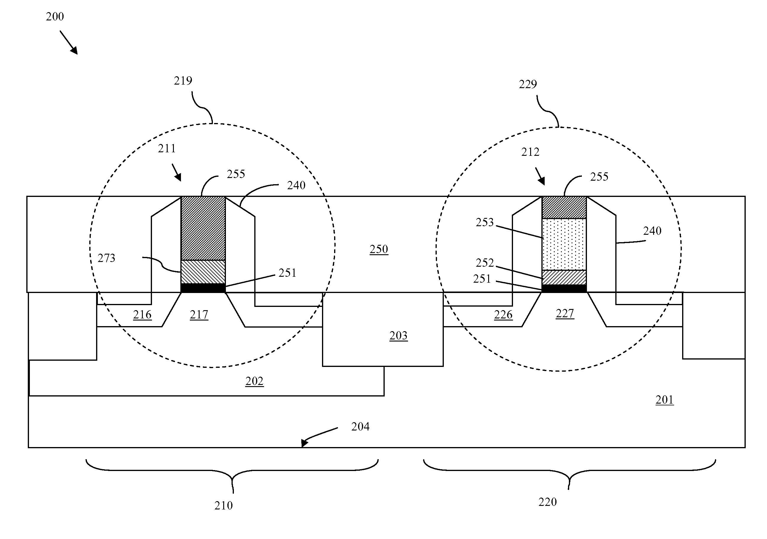
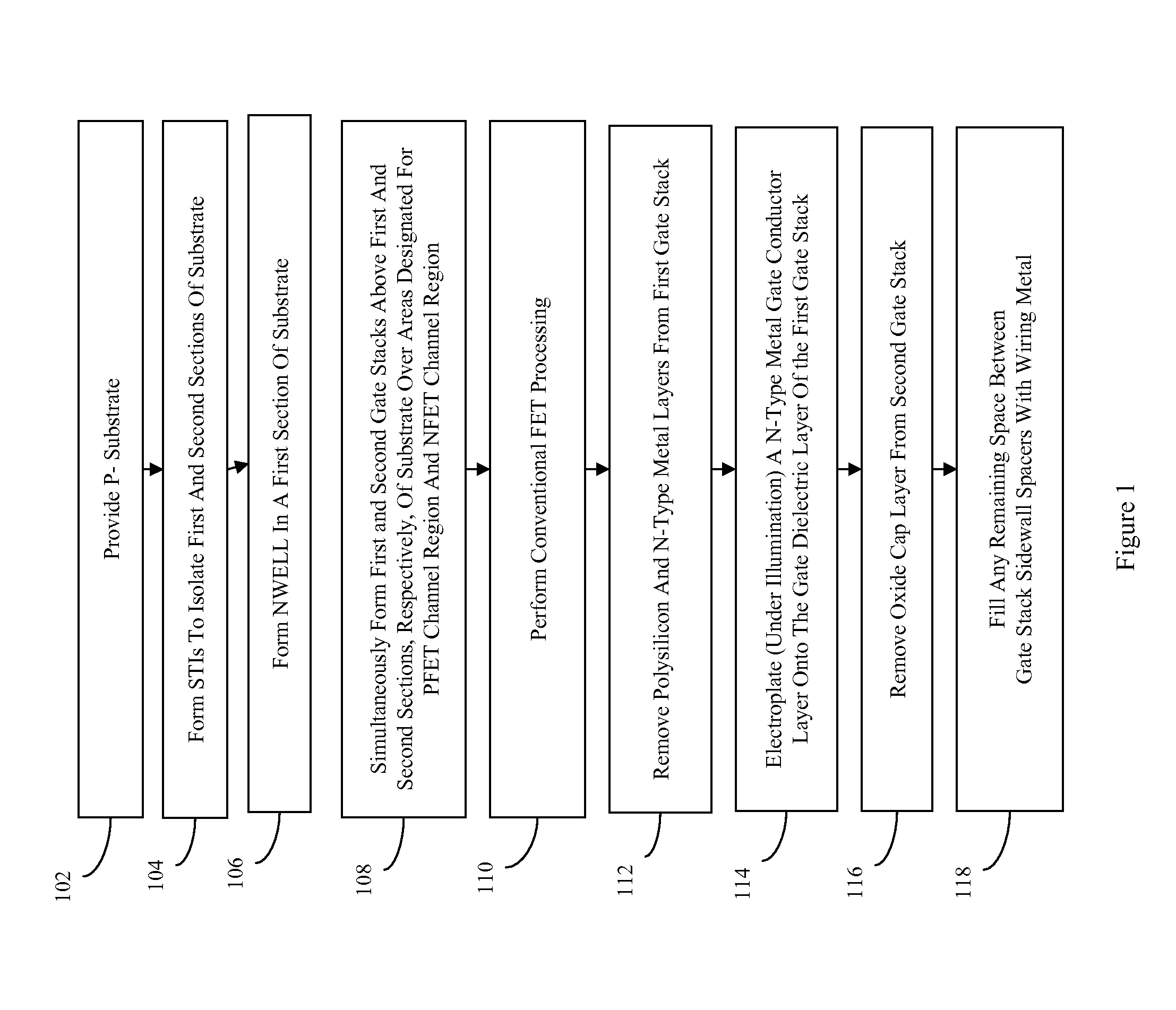
[0037]The embodiments of the invention and the various features and advantageous details thereof are explained more fully with reference to the non-limiting embodiments that are illustrated in the accompanying drawings and detailed in the following description. It should be noted that the features illustrated in the drawings are not necessarily drawn to scale. Descriptions of well-known components and processing techniques are omitted so as to not unnecessarily obscure the embodiments of the invention. The examples used herein are intended merely to facilitate an understanding of ways in which the embodiments of the invention may be practiced and to further enable those of skill in the art to practice the embodiments of the invention. Accordingly, the examples should not be construed as limiting the scope of the embodiments of the invention.

[0038]As mentioned above, prior art complementary metal oxide semiconductor (CMOS) technologies are typically manufactured with a gate stack tha...


PUM


Abstract

Disclosed herein are embodiments of a method of forming a complementary metal oxide semiconductor (CMOS) device that has at least one high aspect ratio gate structure with a void-free and seam-free metal gate conductor layer positioned on top of a relatively thin high-k gate dielectric layer. These method embodiments incorporate a gate replacement strategy that uses an electroplating process to fill, from the bottom upward, a high-aspect ratio gate stack opening with a metal gate conductor layer. The source of electrons for the electroplating process is a current passed directly through the back side of the substrate. This eliminates the need for a seed layer and ensures that the metal gate conductor layer will be formed without voids or seams. Furthermore, depending upon the embodiment, the electroplating process is performed under illumination to enhance electron flow to a given area (i.e., to enhance plating) or in darkness to prevent electron flow to a given area (i.e., to prevent plating).

Description

BACKGROUND[0001]1. Field of the Invention[0002]The embodiments of the invention generally relate to complementary metal oxide semiconductor (CMOS) devices and, more particularly, to a method of forming a CMOS device having an electroplated high-aspect ratio metal replacement gate.[0003]2. Description of the Related Art[0004]Prior art complementary metal oxide semiconductor (CMOS) technologies are typically manufactured with a gate stack that includes a thin silicon oxide (SiO2) gate dielectric layer and a doped-polysilicon gate conductor layer. With device size scaling, the desired gate dielectric thickness has been reduced. Unfortunately, doped polysilicon gate conductors are subject to depletion effects and, thereby increase the effective gate dielectric thickness. Thus, conventional gate structures are not suitable for future CMOS technology generations and, more particularly, for CMOS technology generations beyond the 65 nm node. Rather in order to realize the power requirements...

Claims


Application Information

Patent Timeline
IPC IPC(8): H01L21/8238H01L21/8234
CPCH01L21/823842H01L29/66545H01L29/517
Inventor BASKER, VEERARAGHAVAN S.COTTE, JOHN M.DELIGIANNI, HARIKLIAFURUKAWA, TOSHIHARUPARUCHURI, VAMSI K.TONTI, WILLIAM R.
Owner GLOBALFOUNDRIES INC
Why Eureka
Try Eureka