Enhancement mode III-nitride switch with increased efficiency and operating frequency

a technology of nitride switch and efficiency, applied in the field of high-voltage switching circuit, can solve the problems of the undesirable limitation of efficiency and operating frequency of high-voltage circuits, such as power conversion circuits, by the use of silicon devices, so as to achieve the effect of increasing efficiency and operating frequency

Active Publication Date: 2009-11-12
INFINEON TECH AMERICAS CORP
View PDF9 Cites 115 Cited by
  • Summary
  • Abstract
  • Description
  • Claims
  • Application Information

AI Technical Summary

Benefits of technology

[0007]Enhancement mode III-nitride switch with increased efficiency and operating frequency, substantially as shown in and / or described in connection with at least one of the figures, and as set forth more completely in the claims.

Problems solved by technology

However, the large amount of charge stored by the silicon devices, such as high voltage silicon diodes and transistors, can undesirably limit their efficiency and operating frequency.
Consequently, the efficiency and operating frequency of high voltage circuits, such as power conversion circuits, can be undesirably limited by the use of silicon devices, such as high voltage silicon diodes and transistors, as high voltage switches.

Method used


Image

  • Enhancement mode III-nitride switch with increased efficiency and operating frequency
  • Enhancement mode III-nitride switch with increased efficiency and operating frequency
  • Enhancement mode III-nitride switch with increased efficiency and operating frequency

Examples


Embodiment Construction

[0014]The present invention is directed to an enhancement mode III-nitride switch with increased efficiency and operating frequency. The following description contains specific information pertaining to the implementation of the present invention. One skilled in the art will recognize that the present invention may be implemented in a manner different from that specifically discussed in the present application. Moreover, some of the specific details of the invention are not discussed in order not to obscure the invention.

[0015]The drawings in the present application and their accompanying detailed description are directed to merely exemplary embodiments of the invention. To maintain brevity, other embodiments of the present invention are not specifically described in the present application and are not specifically illustrated by the present drawings.

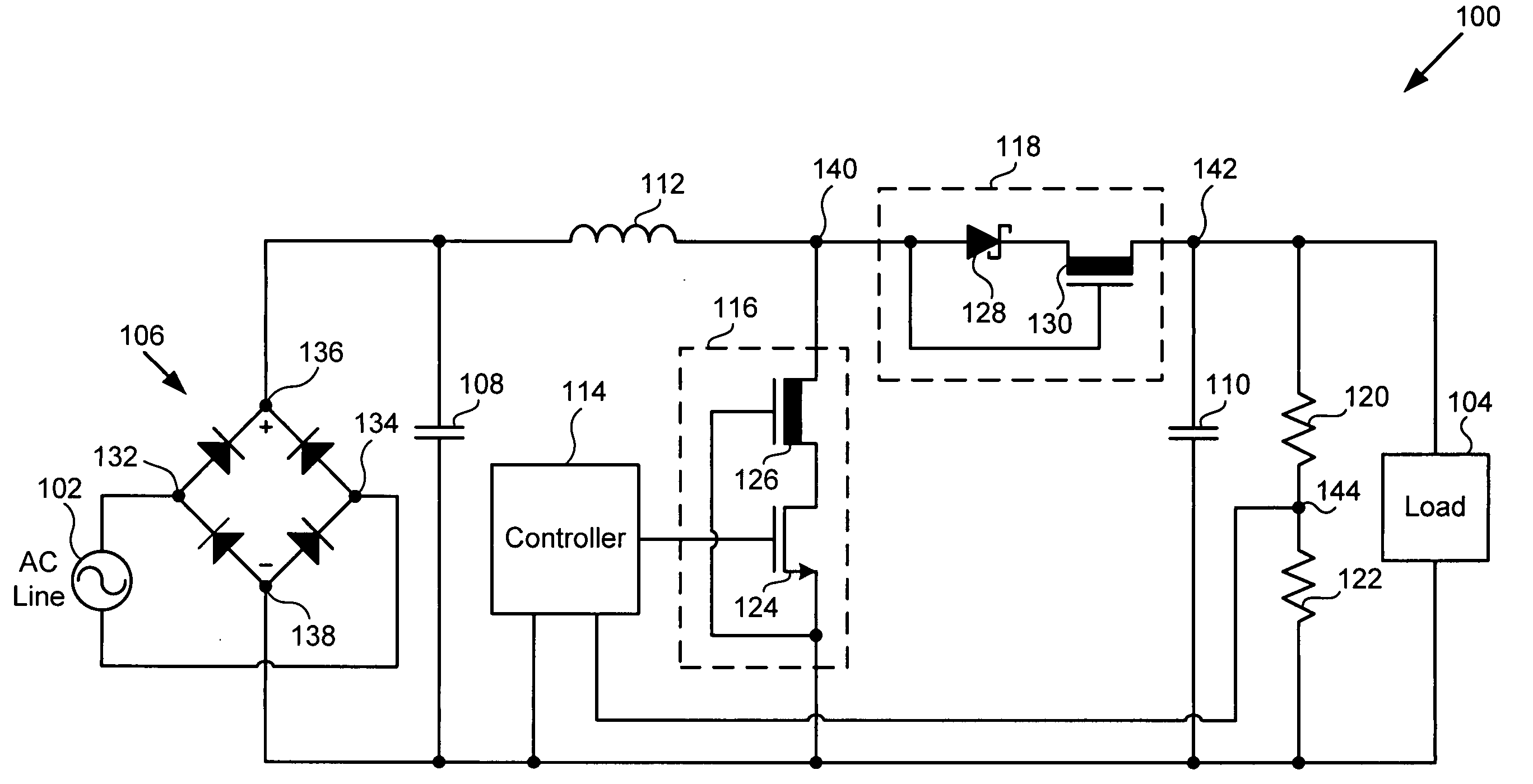
[0016]FIG. 1 shows a circuit diagram of an exemplary power factor correction boost circuit coupled between an AC power source and a lo...


PUM


Abstract

According to one exemplary embodiment, an efficient and high speed E-mode III-N/Schottky switch includes a silicon transistor coupled with a D-mode III-nitride device, where the silicon transistor causes the D-mode III-nitride device to operate in an enhancement mode. The E-mode III-N/Schottky switch further includes a Schottky diode coupled across the silicon transistor so as to improve efficiency, recovery time, and speed of the E-mode III-N/Schottky switch. An anode of the Schottky diode can be coupled to a source of the silicon transistor and a cathode of the Schottky diode can be coupled to a drain of the silicon transistor. The Schottky diode can be integrated with the silicon transistor. In one embodiment the III-nitride device is a GaN device.

Description

[0001]The present application claims the benefit of and priority to a pending provisional patent application entitled “Power Factor Correction Boost Circuit using Enhanced Mode III-Nitride Power Device,” Ser. No. 61 / 050,730 filed on May 6, 2008. The disclosure in that pending provisional application is hereby incorporated fully by reference into the present application.BACKGROUND OF THE INVENTION[0002]1. Field of the Invention[0003]The present invention is generally in the field of switching circuits. More particularly, the invention is in the field of high voltage switching circuits.[0004]2. Background Art[0005]High voltage circuits, such as power conversion circuits, typically require fast switches that are capable of handling high voltages without breaking down. Conventionally, silicon devices, such as high voltage silicon diodes and transistors, have been utilized to provide high voltage switches. For example, a high voltage silicon field effect transistor (FET), such as a high ...

Claims


Application Information

Patent Timeline
Patent Type & Authority Applications(United States)
IPC IPC(8): G05F1/70H01L27/06H01L29/872
CPCH01L21/8258H01L27/0605H01L27/0629H03K2017/6875H03K17/567H03K17/74H03K17/302H01L29/16H01L29/2003
Inventor BAHRAMIAN, TONYZHANG, JASON
Owner INFINEON TECH AMERICAS CORP
Why Eureka
Try Eureka