Integrated biosensing device having photo detector

a biosensor and integrated technology, applied in the field of sensors, can solve the problems of high noise in a fluorescence based optical system, high cost of optical components, and inability to obtain the required sensitivity, so as to improve the above mentioned ratio, reduce the amount of excitation radiation, and improve the effect of integration

Inactive Publication Date: 2009-11-12
KONINKLIJKE PHILIPS ELECTRONICS NV
View PDF8 Cites 17 Cited by
  • Summary
  • Abstract
  • Description
  • Claims
  • Application Information

AI Technical Summary

Benefits of technology

[0010]By providing a reflector according to the invention, a ratio of desired detection of emissions to unwanted detection of the illumination radiation, e.g. illumination light, can be improved. This can be achieved by a reduction in an amount of the illumination reaching the radiation detector, e.g. photodetector, and / or by an increase in the amount of radiation, e.g. illumination, of the sample and thus in the amount of emissions reaching the detector. This can be achieved more cost effectively than by using a wavelength filter. The radiation, e.g. illumination, can be from an external radiation source or in principle it can be provided by a radiation source integrated on the device. The radiation, e.g. illumination, can be visible or invisible wavelengths of the electromagnetic spectrum, according to the type of emissions being stimulated, e.g. far infra red, infra red, visible, ultra violet, far ultraviolet. Likewise the radiation detector, e.g. photodetector, is intended to encompass detectors of visible or invisible wavelengths of the electromagnetic spectrum.
[0013]An additional feature of some embodiments is the device being a single use device. A single use device has the advantage that contamination can be reduced. For such devices it may be more important to keep costs down.
[0016]Another additional feature of some embodiments is a mask over the sample sites and arranged to allow the excitation radiation, e.g. illuminating light, to reach the reflector and to substantially reduce the amount of excitation radiation reaching the detector. This can help improve the above mentioned ratio, or help avoid the need for careful alignment of a narrow beam of the illumination.
[0017]Another such additional feature is two or more reflectors on different sides of the same detector, arranged to deflect radiation, e.g. light, over the same detector. Again this can help improve the above mentioned ratio.
[0018]Another such additional feature is one reflector being arranged to deflect light over more than one detector. This can enable a higher level of integration, or simplify design and manufacture.
[0022]This arrangement enables the radiation detector, e.g. photodetector to face away from a source of external illumination, reducing the need for masking, or other countermeasures.

Problems solved by technology

The fluorescence detection systems used in bench-top / laboratory machines furthermore generally require expensive optical components to acquire and analyse the fluorescence signals.
In particular, expensive optical filters with sharp wavelength cut-off, i.e. filters that are highly selective, are used to obtain the needed sensitivity of these optical systems, as often the shift between the excitation spectrum (absorption) and emission spectrum (fluorescence) is small (<50 nm).
Consequently, the main sources of noise in a fluorescence based optical system are reflection of (a part of) the excitation light and (Rayleigh) scattering of the excitation light.
Having the optical sensor as part of the bench-top machine demands the mounting of a specific filter set for a specific assay, which hampers the parallel (multiplexed) detection of fluorescent labels with various excitation and / or emission spectra.
Nevertheless, the need for filters makes such biochips expensive, which is especially disadvantageous if disposable biochips are considered.
The detection system uses an expensive filter for filtering out the excitation light, whereby the detection sensitivity is limited due to the filtering.

Method used


Image

  • Integrated biosensing device having photo detector
  • Integrated biosensing device having photo detector
  • Integrated biosensing device having photo detector

Examples


Embodiment Construction

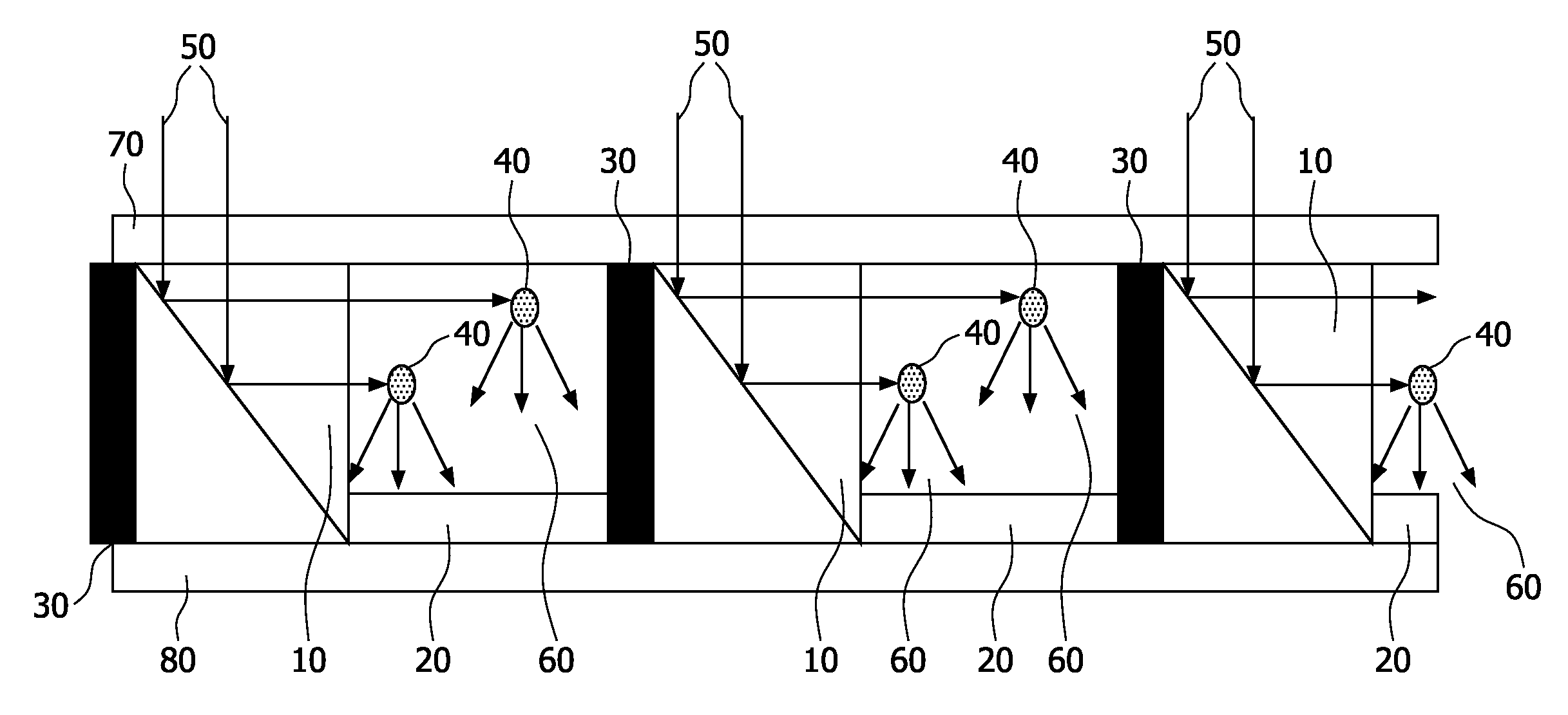
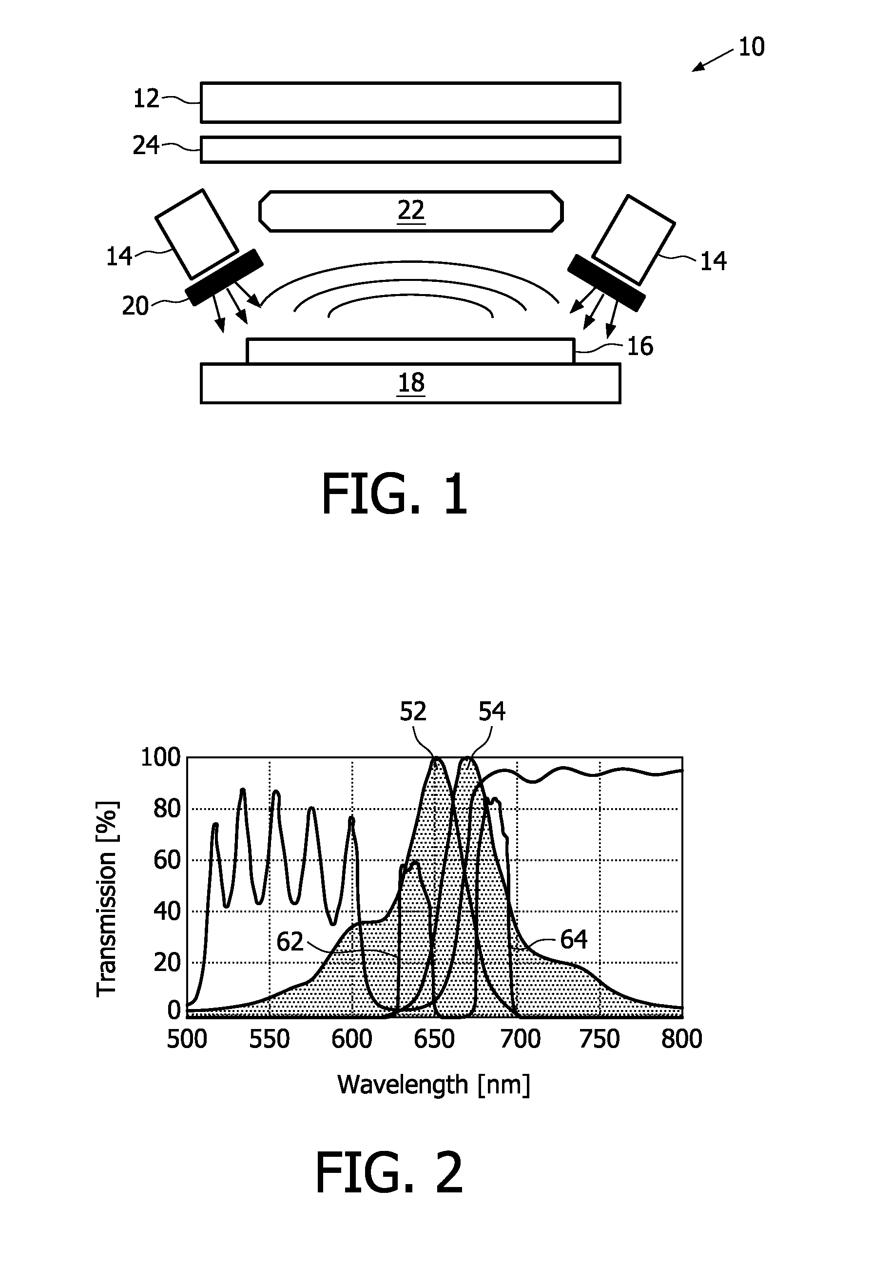
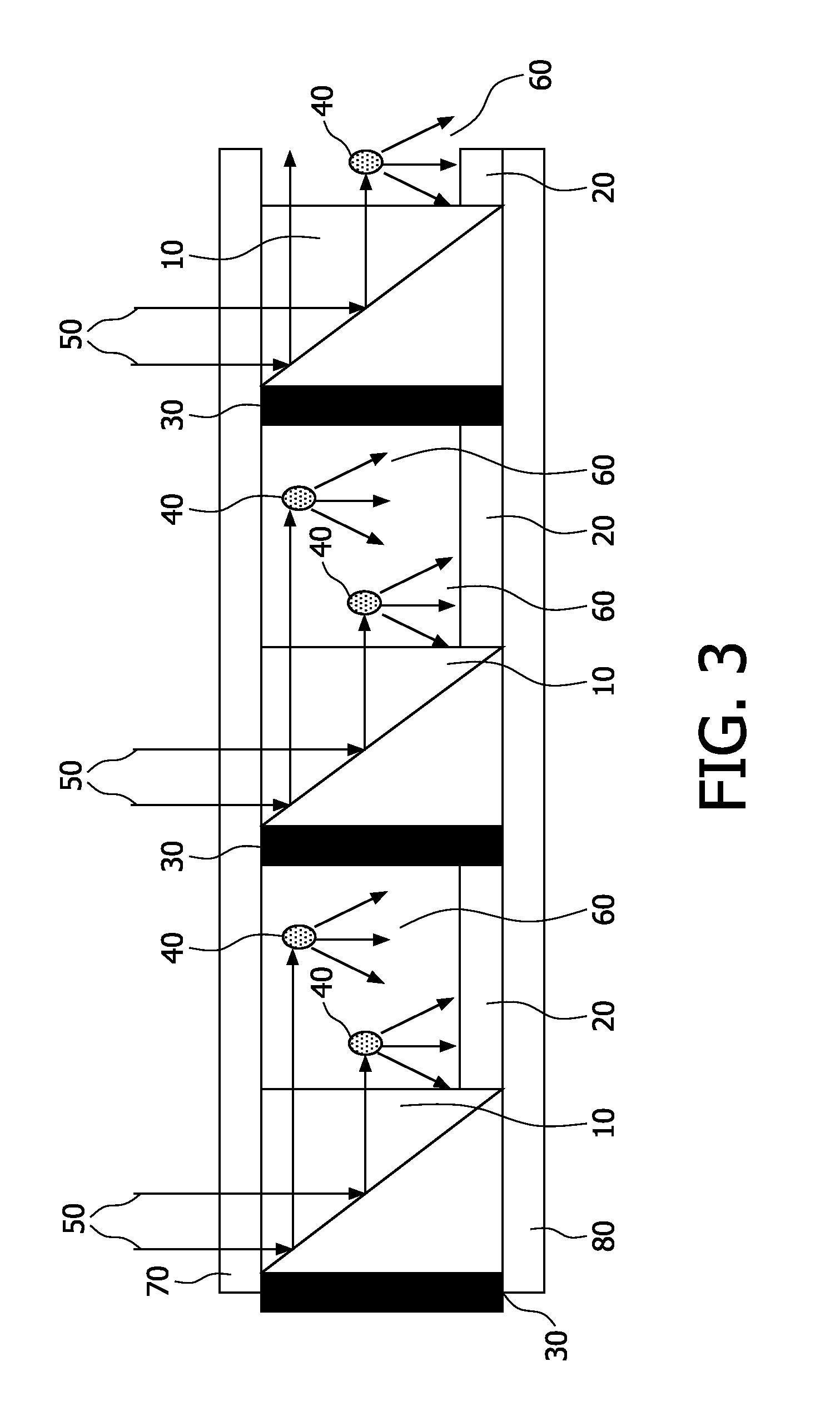
[0036]The present invention will be described with respect to particular embodiments and with reference to certain drawings but the invention is not limited thereto but only by the claims. Any reference signs in the claims shall not be construed as limiting the scope. The drawings described are only schematic and are non-limiting. In the drawings, the size of some of the elements may be exaggerated and not drawn on scale for illustrative purposes. Where the term “comprising” is used in the present description and claims, it does not exclude other elements or steps. Where an indefinite or definite article is used when referring to a singular noun e.g. “a” or “an”, “the”, this includes a plural of that noun unless something else is specifically stated.

[0037]Furthermore, the terms first, second, third and the like in the description and in the claims, are used for distinguishing between similar elements and not necessarily for describing a sequential or chronological order. It is to be...


PUM

PropertyMeasurementUnit
areaaaaaaaaaaa
transparentaaaaaaaaaa
evanescent field excitationaaaaaaaaaa

Abstract

An integrated biosensing device detects emissions from a sample when illuminated. A photo detector (20) is adjacent a site for retaining the sample (40) or receiving excitation radiation for impingement on the sample (40). A reflector (10) deflects the illumination onto the sample site and substantially guides the excitation radiation away from the photo detector. By providing a reflector, a ratio of desired detection of emissions to unwanted detection of the illumination light can be improved. This can be achieved by a reduction in an amount of the illumination reaching the photo detector, and / or by an increase in the amount of illumination of the sample and thus in the amount of emissions reaching the detector. This can be achieved more cost effectively than by using a filter. The illumination can be from above or below if the substrate is transparent.

Description

FIELD OF THE INVENTION[0001]This invention relates to sensors, especially biosensors and to integrated semiconductor devices having a radiation detector such as a photodetector arranged to detect emissions from a sample, and to corresponding methods of manufacturing and using such devices. The present invention also relates to arrays of radiation detectors such as a photodetector and arrays of sample sites, and to corresponding methods of manufacturing and using such arrays.BACKGROUND OF THE INVENTION[0002]Micro-fluidic devices are at the heart of most biochip technologies, being used for both the preparation of fluidic, e.g. blood based, samples and their subsequent analysis. Integrated devices comprising biosensors and micro-fluidic devices are known, e.g. under the name DNA / RNA chips, BioChips, GeneChips and Lab-on-a-chip. In particular, high throughput screening on arrays, e.g. micro-arrays, is one of the new tools for chemical or biochemical analysis, for instance employed in d...

Claims


Application Information

Patent Timeline
Patent Type & Authority Applications(United States)
IPC IPC(8): G01N21/25G01N21/64B23P11/00
CPCB01J2219/00576Y10T29/49826B01L3/502707B01L3/502715B01L2300/0654B01L2300/0816B01L2300/0819B01L2300/1827G01N21/6428G01N21/6454G01N21/648G01N2021/0307G01N2021/7786G01N2201/0221G01N2201/0636G01N2201/064B01J2219/00702
Inventor VAN HERPEN, MAARTEN MARINUS JOHANNES WILHELMUSKLUNDER, DERK JAN WILFREDBALISTRERI, MARCELLO LEONARDO MARIOJOHNSON, MARK THOMASPONJEE, MARC WILHELMUS GIJSBERT
Owner KONINKLIJKE PHILIPS ELECTRONICS NV
Why Eureka
Try Eureka