Ceramic electronic component and method for manufacturing the same

a technology of ceramic electronic components and manufacturing methods, applied in the direction of capacitor manufacturing, fixed capacitor details, fixed capacitors, etc., can solve the problems of less acceptable use of lead-containing solder, cracks or fractures in ceramic element assemblies, and certain hazardous substances in electrical and electronic equipment, so as to achieve excellent heat resistance or reliability

Active Publication Date: 2009-12-03
MURATA MFG CO LTD
View PDF6 Cites 67 Cited by
  • Summary
  • Abstract
  • Description
  • Claims
  • Application Information

AI Technical Summary

Benefits of technology

[0020]In the ceramic electronic component according to a preferred embodiment of the present invention, the external electrode and the metal terminal are preferably directly diffusion-bonded by diffusion of the metal in the metal terminal into the external electrode, and thus metal terminal bonding excellent in heat resistance or reliability can be achieved.

Problems solved by technology

Thus, when a stress is applied to a ceramic electronic component, fractures or cracks may occur in ceramic element assemblies.
However, in recent years, the restriction of the use of certain hazardous substances in electrical and electronic equipment has rapidly proceeded as typified by the European RoHS directive or the like, and the use of a solder containing lead is becoming less acceptable.
However, as disclosed in Japanese Unexamined Patent Application Publication No. 4-259205 and Japanese Unexamined Patent Application Publication No. 2003-303736, when external electrodes and metal terminals are soldered to each other, there has been a problem in that bonding reliability decreases due to insufficient reflow heat resistance when mounting on a substrate, deterioration of a solder itself or deterioration due to the generation of an intermetallic compound at a bonding interface under a high temperature environment or a thermal-cycle environment.

Method used


Image

  • Ceramic electronic component and method for manufacturing the same
  • Ceramic electronic component and method for manufacturing the same
  • Ceramic electronic component and method for manufacturing the same

Examples


first preferred embodiment

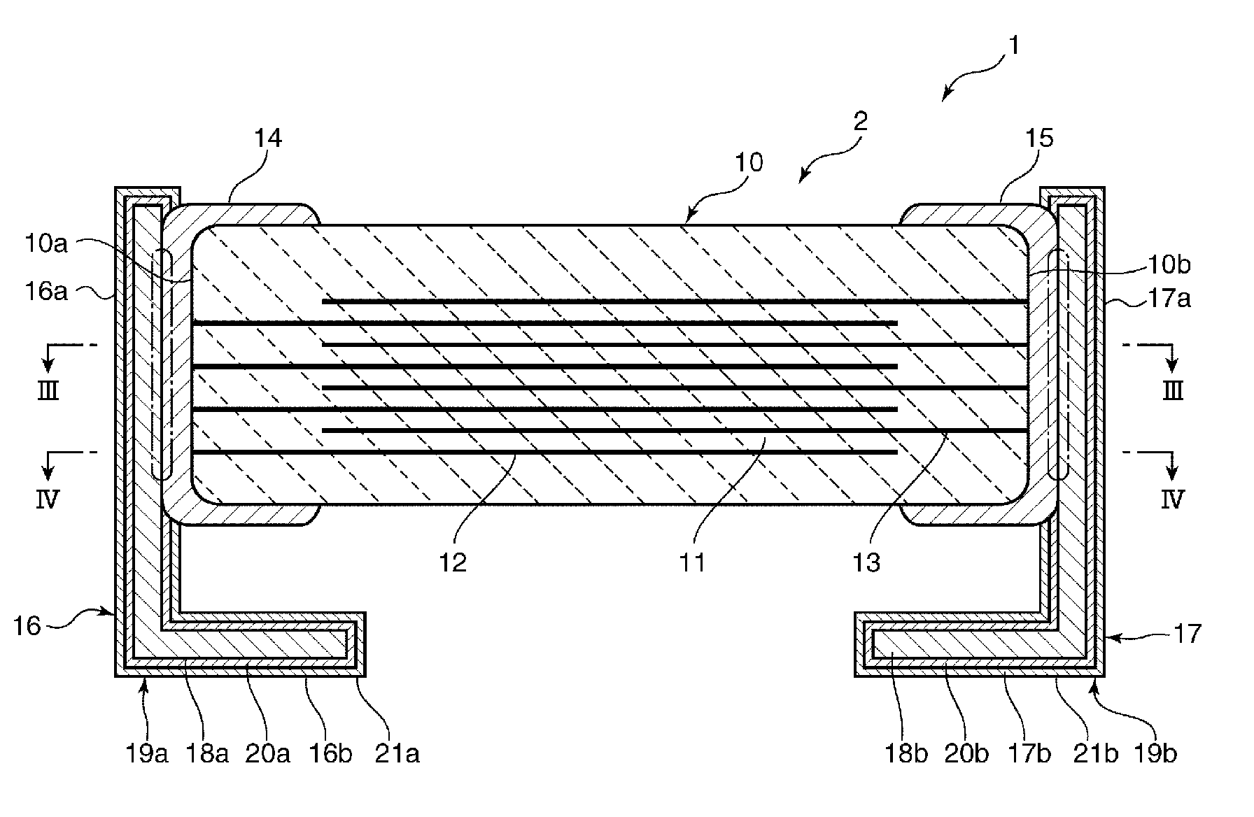
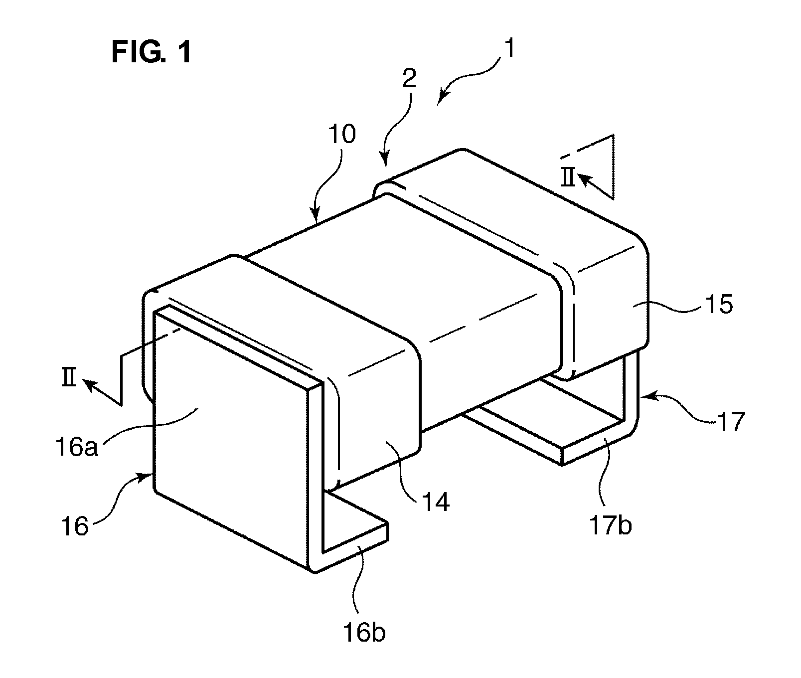
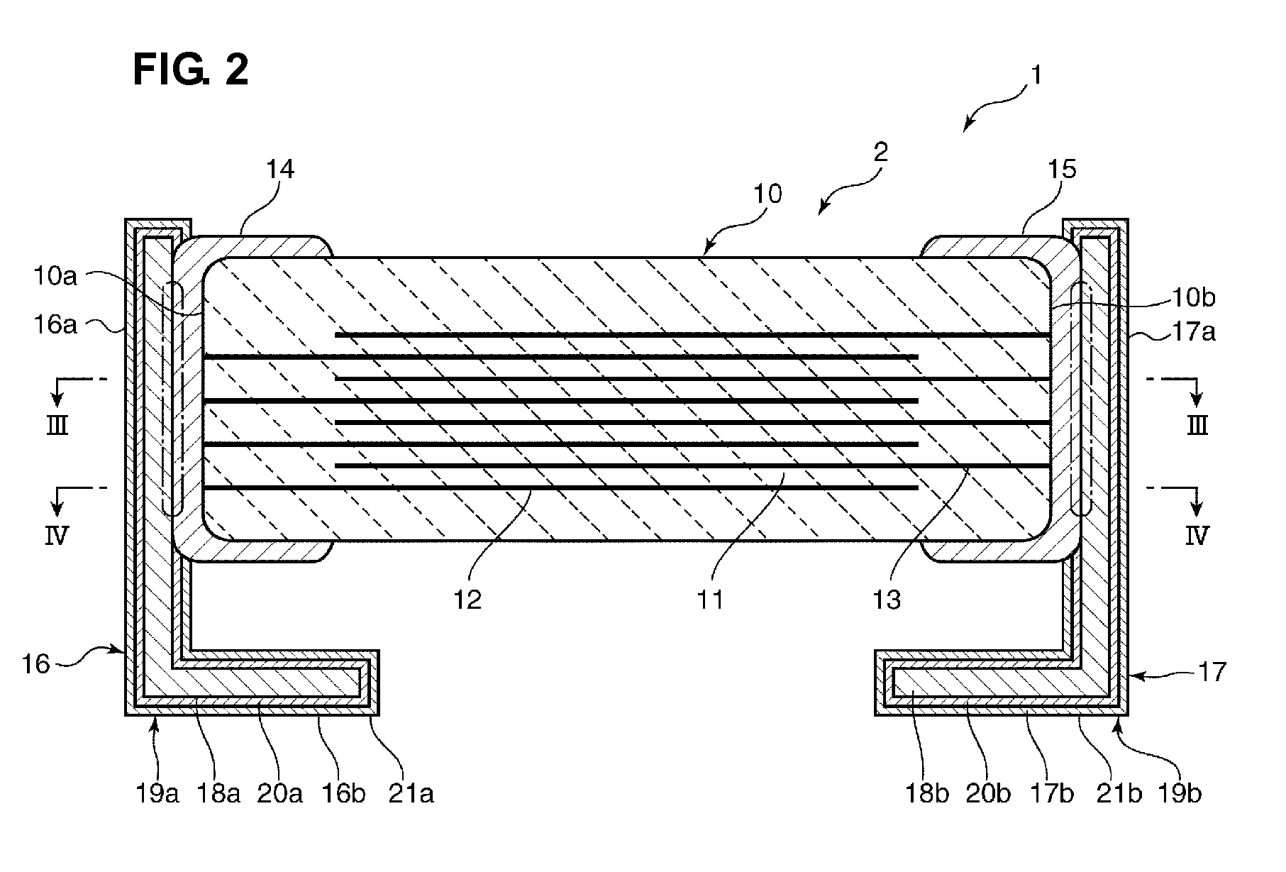
[0043]As shown in FIGS. 1 and 2, a ceramic electronic component 1 has a ceramic element 2 and a pair of metal terminals 16 and 17. The ceramic element 2 has a ceramic element assembly 10 preferably having a substantially rectangular parallelepiped shape which has been R-chamfered, for example. As shown in FIG. 2, the ceramic element assembly 10 has a plurality of laminated ceramic layers 11, and a plurality of first internal electrodes 12 preferably having a substantially rectangular shape and a plurality of second internal electrodes 13 having a substantially rectangular shape disposed between the dielectric layers.

[0044]The ceramic layer 11 is formed using a suitable ceramic. For example, when the ceramic electronic component 1 is a capacitor, the ceramic layer 11 is formed using a dielectric ceramic, such as a BaTiO3 ceramic. For example, when the ceramic electronic component 1 is a piezoelectric component, the ceramic electronic component 1 is formed using a piezoelectric cerami...

first modified example

[0077]The first preferred embodiment describes an example where a pair of bonding terminals 25a and 25b are used for the diffusion-bonding of the first and second external electrodes 14 and 15 with the first and second metal terminals 16 and 17, respectively, as shown in FIG. 6. The bonding terminals used for the diffusion-bonding of the first and second external electrodes 14 and 15 with the first and second metal terminals 16 and 17, respectively, are not limited to the bonding terminals 25a and 25b.

[0078]For example, as shown in FIG. 7, the first and second external electrodes 14 and 15 and the first and second metal terminals 16 and 17 may also be diffusion-bonded using a bonding terminal 27 having a resistive portion 26. Specifically, the bonding terminal 27 has a first terminal portion 28a and a second terminal portion 28b. The tip of the first terminal portion 28a and the tip of the second terminal portion 28b are connected by the resistive portion 26. Therefore, when a curr...

second preferred embodiment

[0082]As shown in FIG. 8, the first metal terminal 16 and the first external electrode 14 may be bonded to each other at a plurality of bonding portions C. Similarly, the second metal terminal 17 and the second external electrode 15 may be bonded to each other at a plurality of bonding portions C. Specifically, in this preferred embodiment, the first and second metal terminals 16 and 17 and the first and second external electrodes 14 and 15 are bonded to each other, respectively, at two bonding portions C.

[0083]When the first metal terminal 16 and the first external electrode 14 are bonded to each other at two bonding portions C, the first metal terminal 16 and the first external electrode 14 can be bonded to each other using a bonding terminal 29 shown in FIG. 9. The bonding terminal 29 has the first and second terminal portions 28a and 28b, first and second resistive portions 30a and 30b, and a bonding portion 31. When the first metal terminal 16 and the first external electrode 1...


PUM

PropertyMeasurementUnit
thicknessaaaaaaaaaa
thicknessaaaaaaaaaa
temperatureaaaaaaaaaa

Abstract

A ceramic electronic component has a ceramic element assembly, external electrodes, and metal terminals. The external electrodes are arranged on the surface of the ceramic element assembly. The external electrodes contain a sintered metal. The metal terminals are electrically connected to the external electrodes, respectively. The external electrode and the metal terminal are directly diffusion-bonded by diffusion of metal in the metal terminals into the external electrodes. The above arrangement provides a ceramic electronic component having highly reliable metal particle bonding and a method for manufacturing the same.

Description

BACKGROUND OF THE INVENTION[0001]1. Field of the Invention[0002]The present invention relates to a ceramic electronic component, and more particularly to a ceramic electronic component having external electrodes and metal terminals electrically connected to the external electrodes, and a method for manufacturing the same.[0003]2. Description of the Related Art[0004]In general, ceramic electronic components, such as a ceramic capacitor, are placed in an environment in which they are easily subjected to a mechanical stress in mounting or during use. For example, a stress is applied to a ceramic electronic component in some cases when a wiring board on which the ceramic electronic component has been mounted bends or when the temperature of the wiring board changes to change the volume of a wiring board due to thermal expansion, for example. Thus, when a stress is applied to a ceramic electronic component, fractures or cracks may occur in ceramic element assemblies. In view of such prob...

Claims


Application Information

Patent Timeline
Patent Type & Authority Applications(United States)
IPC IPC(8): H01G4/228H01G13/00H01G2/06H01G4/232H01G4/30
CPCH01G2/065H01G4/232Y10T29/43H05K3/3426H01G4/30H01G4/2325H01G4/12
Inventor OTSUKA, HIDEKIYOSHIDA, KAZUHIROSONOYAMA, JUNITAGAKI, YOJINAKATA, AKIHIKO
Owner MURATA MFG CO LTD
Why Eureka
Try Eureka