Crystalline nobel metal nanostructures and methods for their preparation

a technology of metal nanostructures and nanostructures, which is applied in the direction of crystal growth process, transportation and packaging, under a protective fluid, etc., can solve the problems of inability to achieve the effect of enhancing the diffraction from the 100 plane, limiting the quantity of nanostructures that can be produced in each run of synthesis, and affecting the fundamental study and device fabrication

Inactive Publication Date: 2009-12-03
UNIV OF WASHINGTON
View PDF3 Cites 26 Cited by
  • Summary
  • Abstract
  • Description
  • Claims
  • Application Information

AI Technical Summary

Benefits of technology

[0035]FIG. 5 is the XRD pattern taken from Pd nanobars shown in FIG. 2B. All the peaks can be indexed to fcc palladium (JCPDS card, 05-0681). No peaks were observed for impurities such as PdBr2 and PdO. The ratio between the intensities of (111) and (200) peaks is much lower than the value reported for a conventional powder sample (1.33 versus 2.38), indicating that the diffraction from {100} planes is enhanced for the sample of nanobars. It is likely that the nanobars preferentially lay on the substrate against their flat {100} facets. As a result, there was a texturing effect. The ED pattern (inset) taken from an assembly of Pd nanobars also indicate that they were highly crystalline. The rings can be indexed to the diffraction from {111}, {200}, {220} and {311} planes of fcc palladium, respectively.

Problems solved by technology

However, polycrystalline wires containing gaps between adjacent grains often shrink alter initial exposure to hydrogen and may cause random, irreversible changes to the resistance of a sensing device.
Although a template-directed synthesis can be very simple and straightforward, it is limited in terms of the quantity of nanostructures that can be produced in each run of synthesis.
It often yields polycrystalline nanostructures, which are less valuable for both fundamental study and device fabrication.
As a result, it seems to be impractical to rely on template-directed synthesis if one needs single-crystal, 1-D nanostructures of palladium.
However, it is not easy to grow 1-D nanostructures of palladium in a solution phase.

Method used


Image

  • Crystalline nobel metal nanostructures and methods for their preparation
  • Crystalline nobel metal nanostructures and methods for their preparation
  • Crystalline nobel metal nanostructures and methods for their preparation

Examples


example 1

Synthesis of Representative Palladium Nanostructures:

Nanorods having an Aspect Ratio of 8

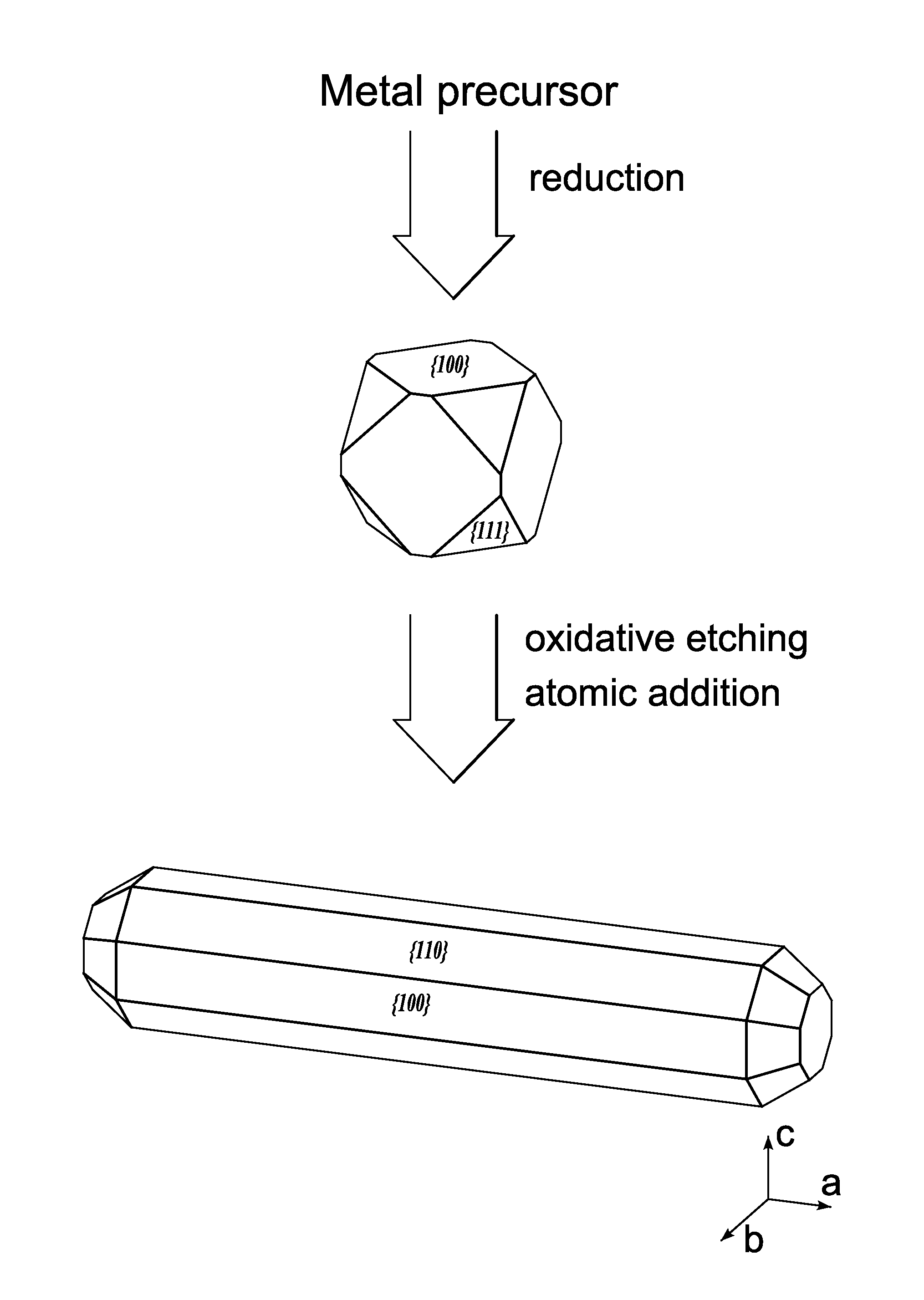
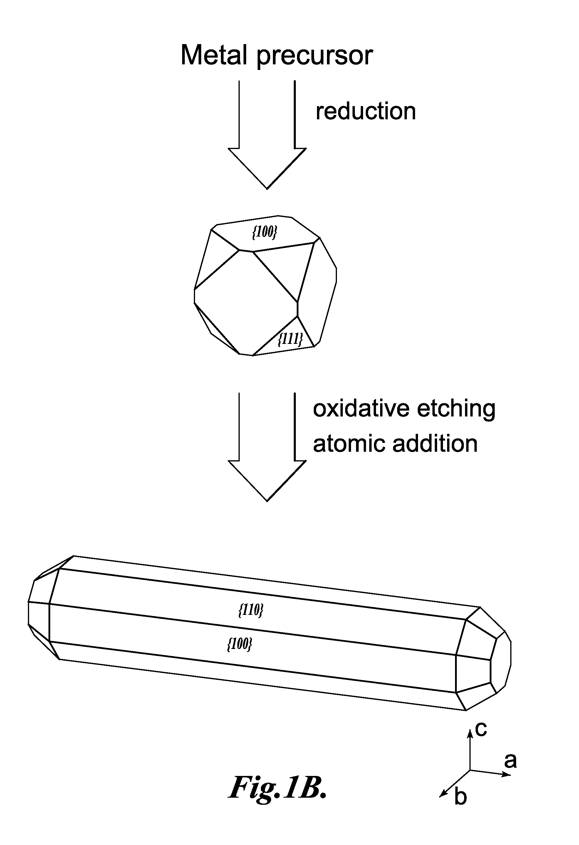
[0104]In this example, the synthesis of representative palladium nanostructures of the invention are described: nanorods having an aspect ratio of about 8.

[0105]In a typical synthesis, 5 mL of EG was hosted in a 25-mL, three-neck flask (equipped with a reflux condenser and a Teflon-coated magnetic stirring bar) and heated in air under magnetic stirring at 100° C. Meanwhile, 0.0486 g of Na2PdCl4 and 0.600 g of KBr were dissolved in 3 mL of water, and 0.0916 g of PVP was dissolved in 3 mL of EG at room temperature. These two solutions (with the molar ratio of PdCl42 to Br− and the repeating unit of PVP being 1:30:15) were then injected simultaneously into the flask using a two-channel syringe pump (KDS200, Stoelting, Wood Dale, Ill.) at a rate of 45 mL per hour. The reaction mixture was heated at 100° C. in air for 1 h before the product was collected by centrifugation and washed with acetone once...

example 2

Synthesis of Representative Palladium Nanostructures:

Nanobars having Aspect Ratios of 2 to 4

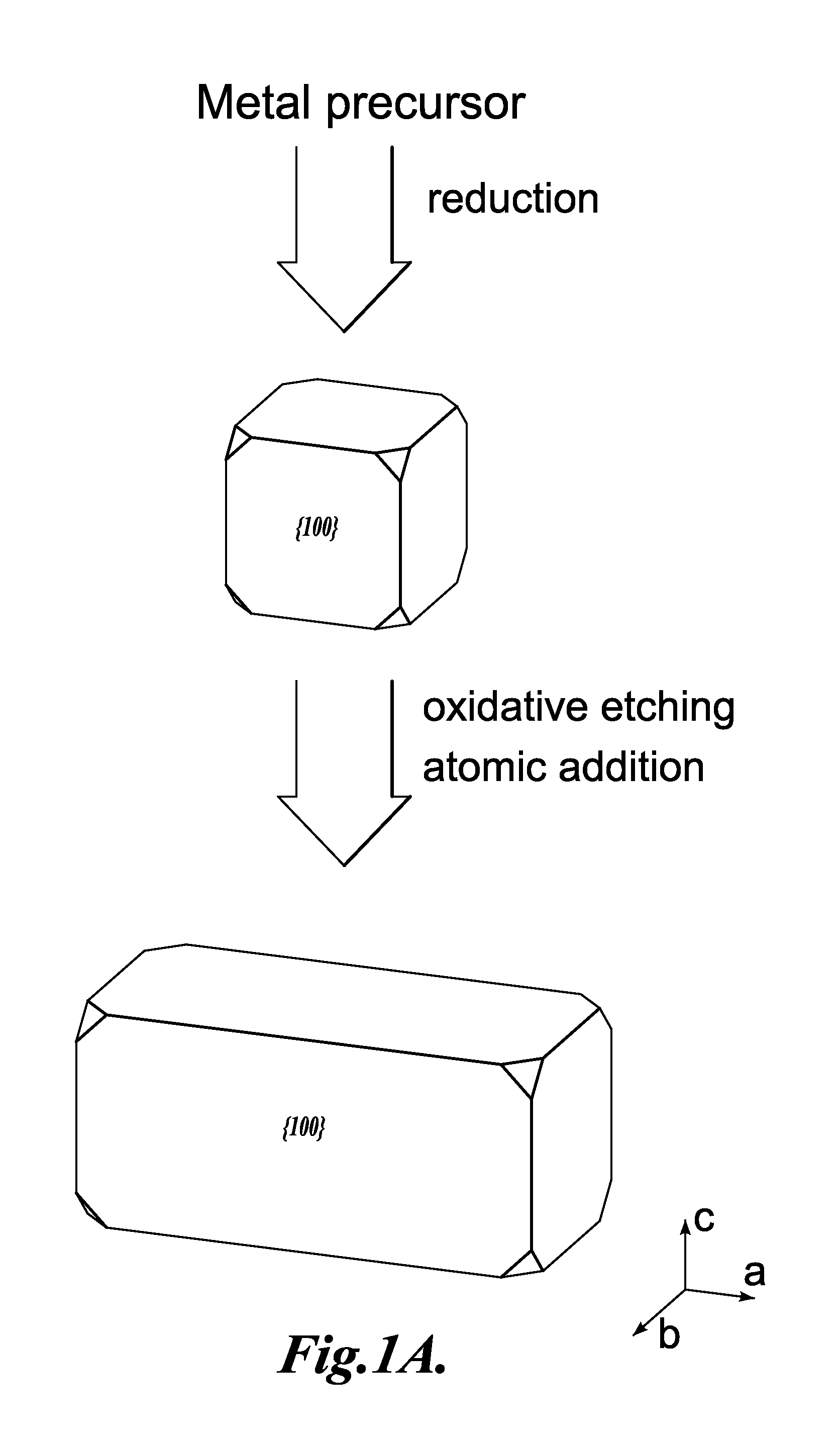
[0106]In this example, the synthesis of representative palladium nanostructures of the invention are described: nanobars having aspect ratios of from about 2 to about 4.

[0107]The procedure was similar to that described above in Example 1 for palladium nanorods, except that the PVP was dissolved in 3 mL of water instead of EG.

example 3

Synthesis of Representative Palladium Nanostructures:

Nanobars having Aspect Ratios of 1 to 1.2

[0108]In this example, the synthesis of representative palladium nanostructures of the invention are described: nanobars having aspect ratios of from about 1 to about 1.2.

[0109]The procedure was similar to that described above in Example 1 for palladium nanorods, except that the solvent for all solutions was water instead of EG. In this case, the hydroxyl end group of PVP served as the reducing agent.


PUM

PropertyMeasurementUnit
aspect ratioaaaaaaaaaa
aspect ratiosaaaaaaaaaa

Abstract

Crystalline noble metal nanostructures and methods for their preparation.

Description

CROSS-REFERENCE TO RELATED APPLICATION[0001]This application claims the benefit of U.S. Patent Application No. 61 / 033,283, filed Mar. 3, 2008, expressly incorporated herein by reference in its entirety.STATEMENT OF GOVERNMENT LICENSE RIGHTS[0002]This invention was made with Government support under Contract No. DMR-0451788 awarded by the National Science Foundation. The Government has certain rights in the invention.BACKGROUND OF THE INVENTION[0003]Single-crystal, one-dimensional (1-D) nanostructures of palladium are attractive as interconnects for fabricating nanoscale electronic devices. For example, palladium can form reliable and reproducible ohmic contacts with carbon nanotubes (CNTs) because palladium has a relatively high work function and can easily wet the carbon surface. This capability allows one to elucidate the intrinsic properties of CNTs and to maximize the performance of CNT-based devices such as field-effect transistors (FETs). Another important property of Pd is it...

Claims


Application Information

Patent Timeline
Patent Type & Authority Applications(United States)
IPC IPC(8): C30B15/36B22F9/00C22C5/04B22F1/054
CPCB22F1/0018B22F9/24B22F2998/00B82Y30/00B22F2001/0037C30B29/02C30B29/605C30B7/14B22F1/0025B22F1/0553B22F1/054B22F1/0547
Inventor XIA, YOUNANXIONG, YUJIE
Owner UNIV OF WASHINGTON
Why Eureka
Try Eureka