
Shielding of datalines with physical placement based on time staggered access

a dataline and physical placement technology, applied in the field of circuits, can solve the problems of slow data path, slow data path, difficult to obtain the very aggressive ddr3 speed target, etc., and achieve the effect of increasing the complexity of the control circuit and high frequency response performan

Active Publication Date: 2009-12-03
PROMOS TECH INC
View PDF14 Cites 4 Cited by
  • Summary
  • Abstract
  • Description
  • Claims
  • Application Information

AI Technical Summary

Benefits of technology

[0008]According to the present invention, high frequency response performance in data line transmission is achieved without the addition of unnecessary shielding lines and their associated area penalty, or without significantly increased control circuit complexity.

Problems solved by technology

For a one giga-bit DDR3 DRAM the length of the internal data lines is so long that the inherent RC delays make it difficult to obtain the very aggressive DDR3 speed targets.
Thus, the situation where one data line is switching in a given direction surrounded by two data lines switching in the opposite direction results in a very slow data path.
As is shown in FIG. 1, one option to an integrated circuit designer is to use no shields at all, but this “solution” is slow due to the mutual capacitive coupling of adjacent lines switching at the same time.
Running a “shield”, either a ground line or a line known not to be switching when the data lines are switching is one solution that is known to those skilled in the art, but this solution adds numerous extra lines and therefore adds chip area.
Usually there are not enough “DC signal lines” to separate all the data lines, and adding power lines certainly adds area.
This solution leads to no net increase in line slots, but the control and timing of such a scheme has proved difficult.

Method used


Image

  • Shielding of datalines with physical placement based on time staggered access
  • Shielding of datalines with physical placement based on time staggered access
  • Shielding of datalines with physical placement based on time staggered access

Examples


Embodiment Construction

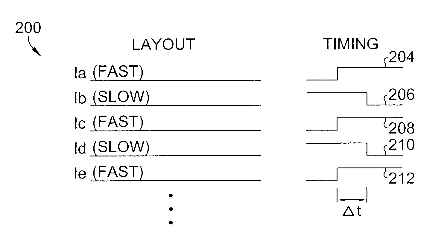
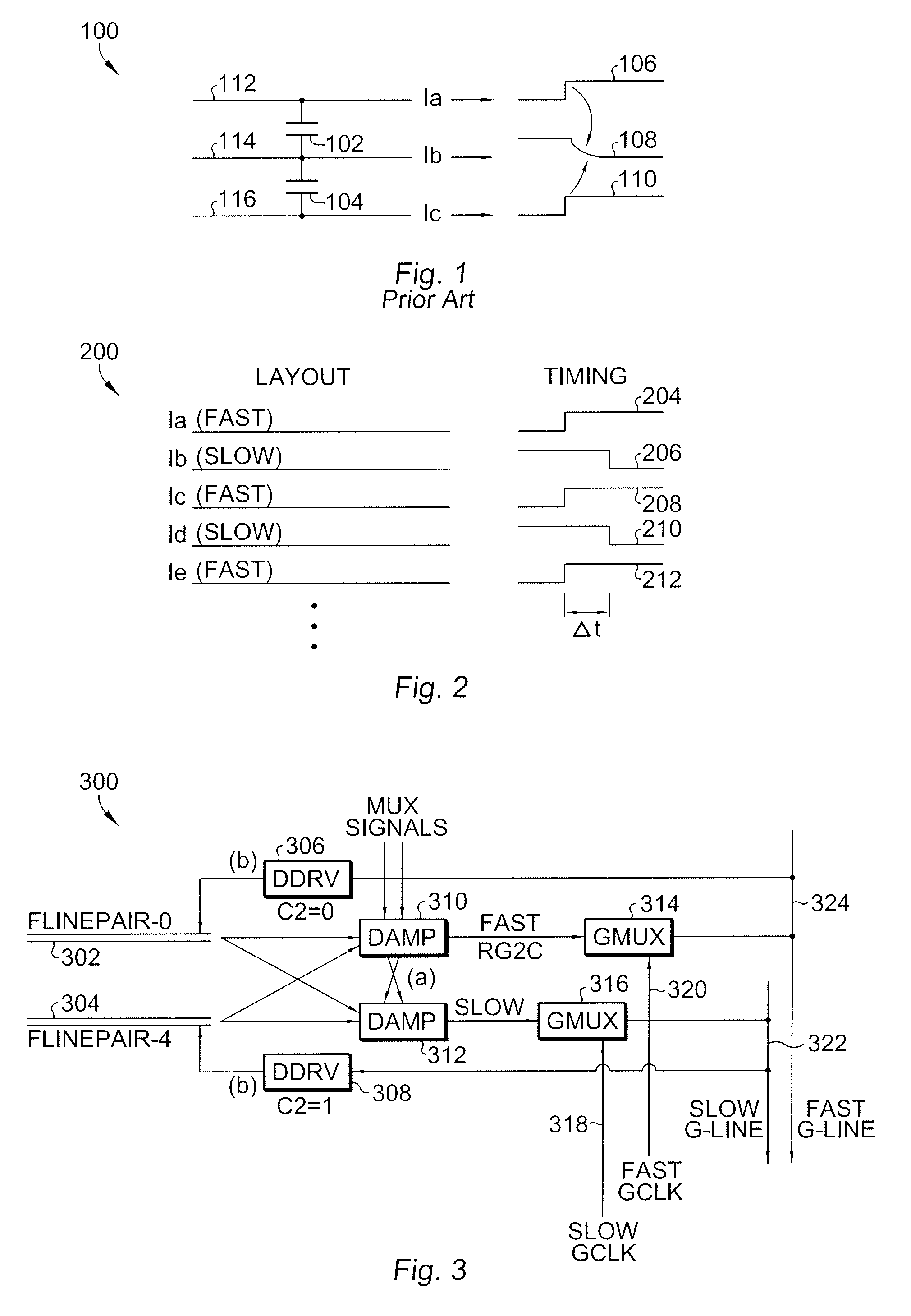
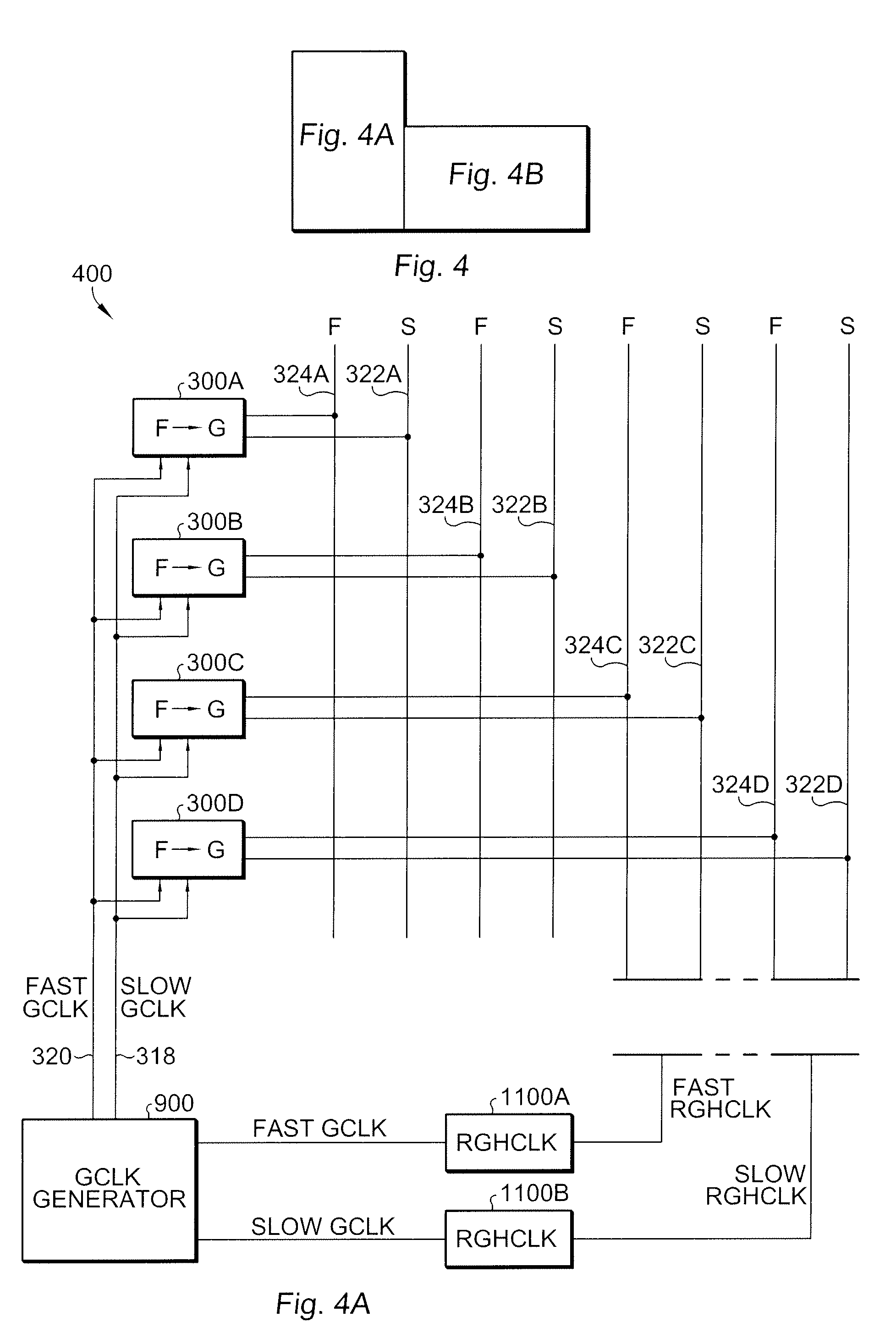
[0022]The present invention uses 128 data lines with no dedicated shields, but relies on the nature of the DDR3 eight bit pre-fetch to split the data bus into two groups: a fast group and a slow group. Since both groups are not switching at the same time, they appear to shield each other as long as they are physically placed in a fast-slow-fast-slow-etc. orientation. Referring now to FIG. 2, a data bus 200 according to the present invention is shown. Lines Ia through Ie alternate, wherein lines Ia, Ic, and Ie are fast data lines, and lines Ib and Id are slow data lines. The corresponding data line waveforms are shown, wherein waveforms 204, 208, and 212 step up first, and then a Δt later, waveforms 206 and 210 step down. Thus, the slow group is switched a Δt after the fast group. This Δt has to be long enough to allow the fast group to have completed switching (roughly 90% of Δv switch), but the Δt must be short enough so the slow data arrives at the output buffer in time. By using ...


PUM


Abstract

A bus driver circuit divides an internal data bus for an integrated circuit memory into at least two groups, designated by speed. A faster group of data lines and a slower group of data lines are placed in an interleaved fashion in order to provide a two group shielding solution. At the earliest opportunity following the reception of a read command, the data from memory banks in the memory is sorted into these two groups. For a DDR3 memory, the sorting method is based on the A2 column address, known as C2. All of the data is brought out of the banks in parallel and sorted as it enters the main amplifiers. These main amplifiers are also divided into two groups, faster and slower. Each amplifier then connects to a data line (G-line) of the same group. The clock assigned to the fast group fires right away, thereby connecting the data associated with the fast amplifiers to the fast data group. This data group then proceeds to the output buffers through the entire data path as fast as possible. The second, slower data group is started with a delayed clock signal and proceeds through the data path to the output buffer maintaining a fixed delay. Since the first and second data groups are not switching at the same time they act as shields to one another.

Description

CROSS REFERENCE TO RELATED PATENT APPLICATIONS[0001]The present invention is related to the subject matter disclosed in U.S. patent application Ser. Nos. 11 / 625,744 filed Jan. 22, 2007 as Attorney Docket No. UMI-375 DIV, for SHIELDED BITLINE ARCHITECTURE FOR DYNAMIC RANDOM ACCESS MEMORY (DRAM) ARRAYS and 11 / 679,632 filed Feb. 27, 2007 as Attorney Docket No. UMI-382 for METHOD TO REGULATE PROPAGATION DELAY OF CAPACITIVELY COUPLED PARALLEL LINES assigned to ProMOS Technologies PTE.LTD, assignee of the present invention, the disclosures of which are herein specifically incorporated by this reference in their entirety.BACKGROUND OF THE INVENTION[0002]The present invention relates to integrated circuit memories and other types of integrated circuits and, more specifically, to a circuit and method for shielding long data lines from one another in the integrated circuit.[0003]For a one giga-bit DDR3 DRAM the length of the internal data lines is so long that the inherent RC delays make it d...

Claims


Application Information

Patent Timeline
Patent Type & Authority Applications(United States)
IPC IPC(8): G06F13/14
CPCG11C7/02G11C7/1006G11C11/4097G11C7/1042G11C11/4096G11C7/1012
Inventor FAUE, JON
Owner PROMOS TECH INC
Learn More