Method and system for post-routing lithography-hotspot correction of a layout

a technology of layout and lithography, applied in the field of semiconductor manufacturing, can solve the problems of increasing the number of lithography “hotspots, the drawback of introducing a large number of false alarms, and the drawback of becoming even more prominen

Active Publication Date: 2009-12-03
SYNOPSYS INC
View PDF3 Cites 52 Cited by
  • Summary
  • Abstract
  • Description
  • Claims
  • Application Information

AI Technical Summary

Benefits of technology

[0013]In a variation on this embodiment, while correcting the lithography hotspot using the correction guidance information, the s...

Problems solved by technology

Many yield and reliability issues can be attributed to certain layout configurations, referred to as “process-hotspots” or “hotspots,” which are susceptible to process issues, such as stress and lithographic process fluctuations.
One of the main yield limiters is the increasing number of lithography “hotspots” that arise from the complexity of design layouts as technology nodes shrink to 65 nm and below.
However, this purely rule-ba...

Method used


Image

  • Method and system for post-routing lithography-hotspot correction of a layout
  • Method and system for post-routing lithography-hotspot correction of a layout
  • Method and system for post-routing lithography-hotspot correction of a layout

Examples


Embodiment Construction

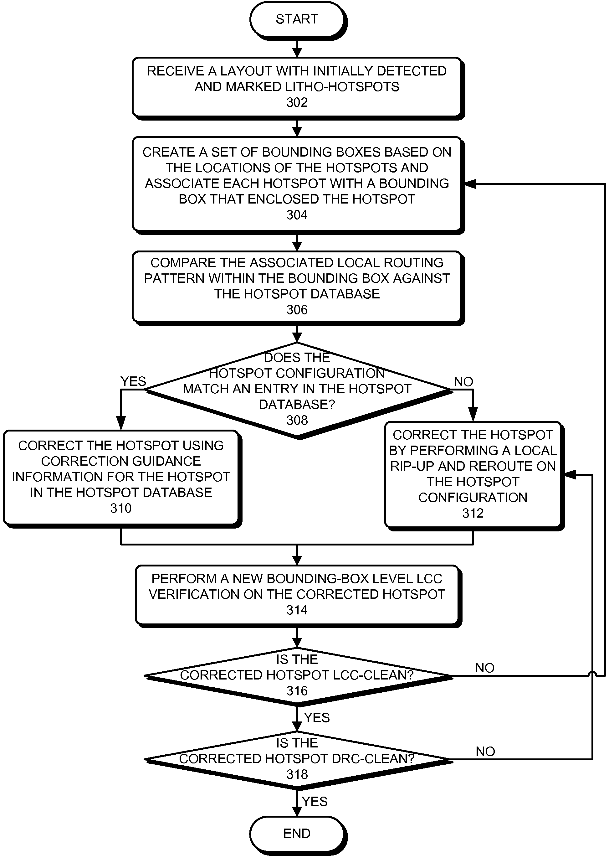
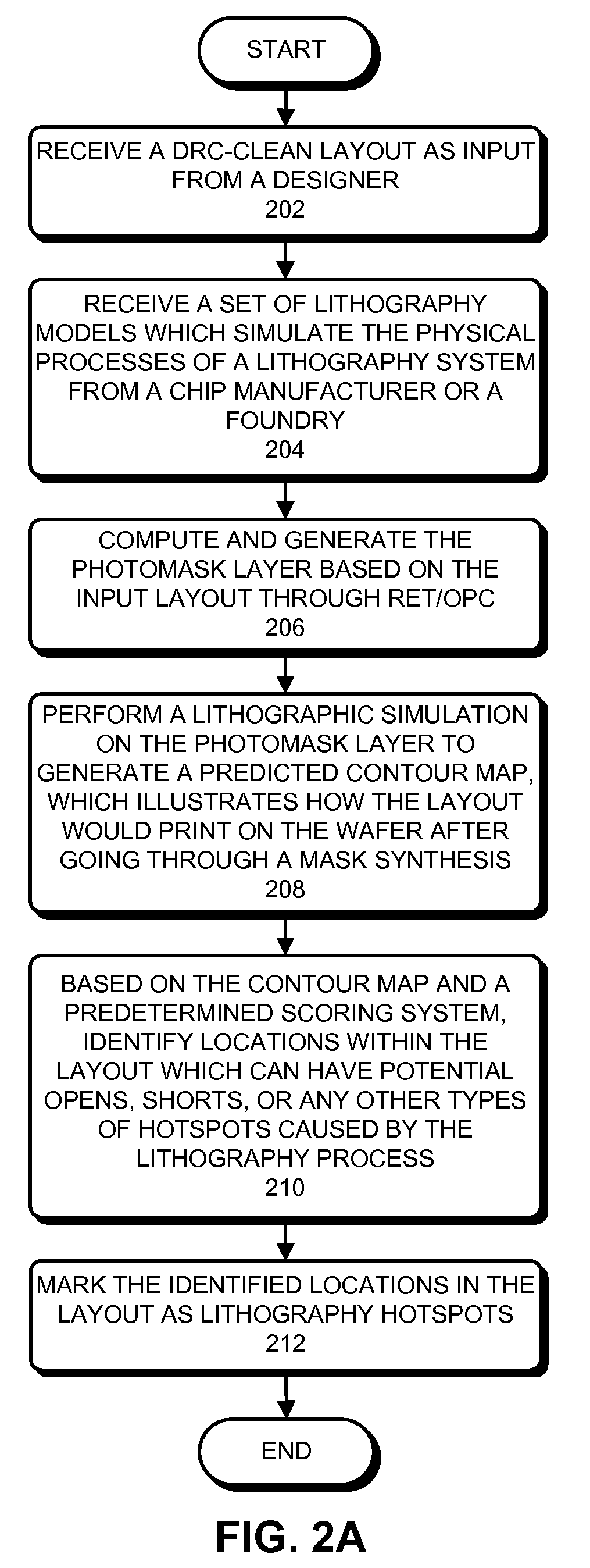
[0027]The following description is presented to enable any person skilled in the art to make and use the invention, and is provided in the context of a particular application and its requirements. Various modifications to the disclosed embodiments will be readily apparent to those skilled in the art, and the general principles defined herein may be applied to other embodiments and applications without departing from the spirit and scope of the present invention. Thus, the present invention is not limited to the embodiments shown, but is to be accorded the widest scope consistent with the claims.

[0028]The data structures and code described in this detailed description are typically stored on a computer-readable storage medium, which may be any device or medium that can store code and / or data for use by a computer system. This includes, but is not limited to, volatile memory, non-volatile memory, magnetic and optical storage devices such as disk drives, magnetic tape, CDs (compact dis...


PUM


Abstract

One embodiment of the present invention provides a system that verifies an integrated circuit (IC) chip layout. During operation, the system receives a layout of an IC chip after the layout has gone through a place-and-route operation. Next, the system performs a lithography compliance checking (LCC) operation on the layout to detect lithography hotspots within the layout, wherein each lithography hotspot is associated with a local routing pattern around the lithography hotspot. Next, for each detected lithography hotspot, the system compares the associated local routing pattern against a hotspot database to determine if the local routing pattern matches an entry in the hotspot database, which stores a set of known hotspot configurations. If so, the system corrects the lithography hotspot using correction guidance information associated with the hotspot configuration stored in the hotspot database. Otherwise, the system corrects the lithography hotspot by performing a local rip-up and reroute on the local routing pattern, iteratively, until achieving convergence or given number of iterations.

Description

BACKGROUND[0001]1. Field of the Invention[0002]Embodiments of the present invention generally relate to semiconductor manufacturing. More specifically, embodiments of the present invention relate to a method and a system for identifying and correcting locations in a routed layout of an integrated circuit (IC) chip that are susceptible to lithography errors.[0003]2. Related Art[0004]Advances in IC manufacturing technology have enabled minimum feature sizes on IC chips to continuously decrease. Meanwhile, manufacturability-aware physical design, which takes into account both yield and reliability during the physical-design process, is becoming increasingly important in bridging the gap between design and manufacturing for nanometer-scale fabrication processes. Many yield and reliability issues can be attributed to certain layout configurations, referred to as “process-hotspots” or “hotspots,” which are susceptible to process issues, such as stress and lithographic process fluctuations...

Claims


Application Information

Patent Timeline
IPC IPC(8): G06F17/50
CPCG03F1/144G06F2217/12G06F17/5081G06F30/398G06F2119/18Y02P90/02
Inventor TONG, YANG-SHANZHANG, DANIELWEI, LINNIMILOSLAVSKY, ALEXTSENG, WEI-CHIHTANG, ZONGWU
Owner SYNOPSYS INC
Why Eureka
Try Eureka