Method of Fabricating Light Emitting Device and Compound Semiconductor Wafer and Light Emitting Device

Inactive Publication Date: 2009-12-10
SHIN-ETSU HANDOTAI CO LTD
View PDF11 Cites 0 Cited by
  • Summary
  • Abstract
  • Description
  • Claims
  • Application Information

AI Technical Summary

Benefits of technology

[0023]When growing the light emitting layer section by the MOVPE method, by using a single crystal substrate which is not off-angled, Group III atoms can not be randomly distributed within the light emitting layer section, so that undesirable regularization or biased distribution of atom arrangement can possibly occur. An area where these regularization and bias occur has a band gap energy value different from one initially expected, so as to distribute band gap energy of the entire light emitting layer section as a result, and then to induce variations of light emitting spectrum profile and center wavelength thereof. However, by providing the single crystal substrate with an appropriate off-angle, the above regulation and bias of the Group III atoms can decrease extensively, and a light emitting device having uniform light emitting spectrum profile and center wavelength can be obtained. Also, when using an off-angled single crystal substrate as a single crystal growth substrate, facet hardly occurs on a surface of the finally-obtained current spreading layer, and a current spreading layer having excellent smoothness can be obtained.
[0024]When composing the light emitting layer section with (AlxGa1-x)yIn1-yP, the single crystal growth substrate can be a GaAs single crystal substrate provided with a principal axis off-angled in a degree range of 10° to 20°, both ends inclusive, while having a <100> direction or a <111> direction as a basic direction. Using a GaAs single crystal off-angled highly like this can improve a polishing effect of a surface of the GaP current spreading layer finally obtained by the Hydride Vapor Pha

Problems solved by technology

However, when a thick current spreading layer is formed at a high rate by using Hydride Vapor Epitaxial Growth Method, crystal defect called hillock is likely to occur on a sur

Method used


Image

  • Method of Fabricating Light Emitting Device and Compound Semiconductor Wafer and Light Emitting Device
  • Method of Fabricating Light Emitting Device and Compound Semiconductor Wafer and Light Emitting Device
  • Method of Fabricating Light Emitting Device and Compound Semiconductor Wafer and Light Emitting Device

Examples


Example

EXAMPLE 1

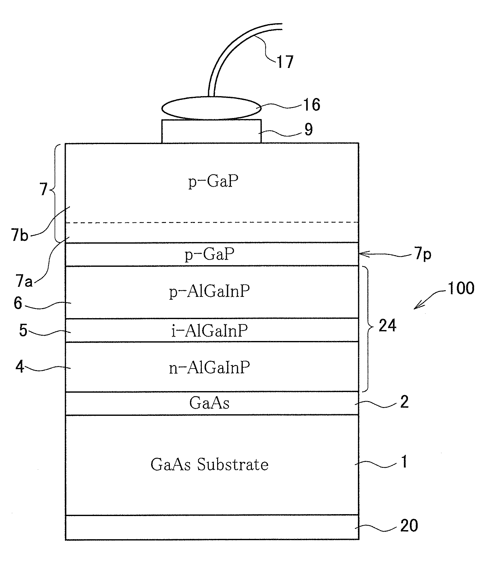
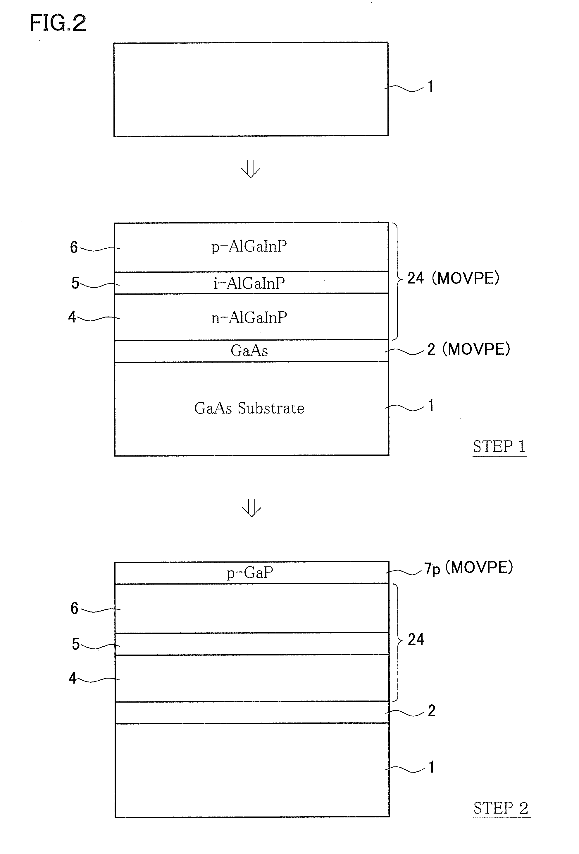
[0052]The compound semiconductor wafer 200 shown in FIG. 3 is formed so that each layer has thickness, as follows. Also, as a GaAs single crystal substrate, one provided with a principal axis off-angled in a degree of approximately 15°, while having a direction as a basic direction is used. An n-type AlGaInP cladding layer 4, an AlGaInP active layer 5, a p-type AlGaInP cladding layer 6 and a GaP connection layer 7p are formed using a MOVPE equipment (Metal Organic Vapor Phase Epitaxy step), and a GaP low-rate growth layer 7a and a GaP high-rate growth layer 7b are formed in hydrogen atmosphere at approximately 760° C. using a Hydride Vapor Phase Epitaxial Growth equipment (Hydride Vapor Phase Epitaxial Growth step), so as to obtain the compound semiconductor wafer 200. The GaP low-rate growth layer 7a is formed at a growth rate of approximately 6 μm / hour, and the GaP high-rate growth layer 7b is formed at a growth rate of approximately 20 μm / hour. Also, thickness of each l...

Example

EXAMPLE 2

[0060]Under the same conditions as Example 1 except that the GaP low-rate growth layer 7a is 2 μm, a compound semiconductor wafer was fabricated by conducting the Metal Organic Vapor Phase Epitaxy step and the Hydride Vapor Phase Epitaxial Growth step similarly. When a main surface of the obtained GaP current spreading layer was visually observed under fluorescent light, hillock was not found. Also, forward voltage (Vf) thereof at 20 mA was approximately 1% higher than that of Example 1.

Example

Comparative Example 1

[0061]Under the same conditions as Example 1 except that the GaP low-rate growth layer 7a is not formed, a compound semiconductor wafer was fabricated by conducting the Metal Organic Vapor Phase Epitaxy step and the Hydride Vapor Phase Epitaxial Growth step. When a main surface of the obtained GaP current spreading layer was visually observed under fluorescent light, hillock was found on an entire surface thereof. Also, forward voltage (Vf) thereof at 20 mA was approximately 1% higher than that of Example 1.


PUM


Abstract

A Metal Organic Vapor Phase Epitaxy step of growing a light emitting layer section 24, composed of a first Group III-V compound semiconductor, epitaxially on a single crystal growth substrate 1 by Metal Organic Vapor Phase Epitaxy, and a Hydride Vapor Phase Epitaxial Growth step of growing a current spreading layer 7 on the light emitting layer section 24 epitaxially by Hydride Vapor Phase Epitaxial Growth Method, are conducted in this order. Then, the current spreading layer 7 is grown, having a low-rate growth layer 7a positioned close to the light emitting layer side and then a high-rate growth layer 7b, having a growth rate of the low-rate growth layer 7a lower than that of the high-rate growth layer 7b, so as to provide a method of fabricating a light emitting device capable of preventing hillock occurrence while forming the thick current spreading layer.

Description

RELATED APPLICATIONS[0001]This application is a National Stage entry of International Application No. PCT / JP2007 / 055476, filed Mar. 19, 2007, and claims the priority of Japanese Patent Application No. 2006-099231 filed on Mar. 31, 2006. The disclosures of the prior applications are hereby incorporated herein in their entirety by reference.BACKGROUND OF THE INVENTION[0002]1. Field of the Invention[0003]This invention relates to a method of fabricating a light emitting device, a compound semiconductor wafer, and a light emitting device.[0004]2. Description of the Related Art[0005][Patent Document 1] U.S. Pat. No. 5,008,718[0006][Patent Document 2] Japanese Laid-Open Patent Publication No. 2004-128452[0007]A light emitting device having a light emitting layer section thereof composed of an (AlxGa1-x)yIn1-yP alloy (where, 0≦x≦1, 0≦y≦1; simply referred to as AlGaInP alloy, or more simply as AlGaInP, hereinafter) can be realized as a high-luminance device, by adopting a double heterostruc...

Claims


Application Information

Patent Timeline
IPC IPC(8): H01L33/00H01L33/14
CPCH01L21/02395H01L21/02433H01L21/02461H01L21/02463H01L21/02505H01L33/14H01L21/02576H01L21/02579H01L21/0262H01L33/0066H01L21/02543
Inventor KUME, FUMITAKASHINOHARA, MASAYUKI
Owner SHIN-ETSU HANDOTAI CO LTD
Why Eureka
Try Eureka