

Analytical scanning evanescent microwave microscope and control stage
a scanning evanescent microwave microscope and scanning probe technology, applied in the field of scanning probe microscopy, can solve the problems of inconvenient control of the probe tip, the inability to accurately perform quantitative conductivity measurements of the test specimen, and the inability to reliably test the accuracy of the test results
- Summary
- Abstract
- Description
- Claims
- Application Information
AI Technical Summary
Benefits of technology
Problems solved by technology
Method used
Image

Examples
embodiment a
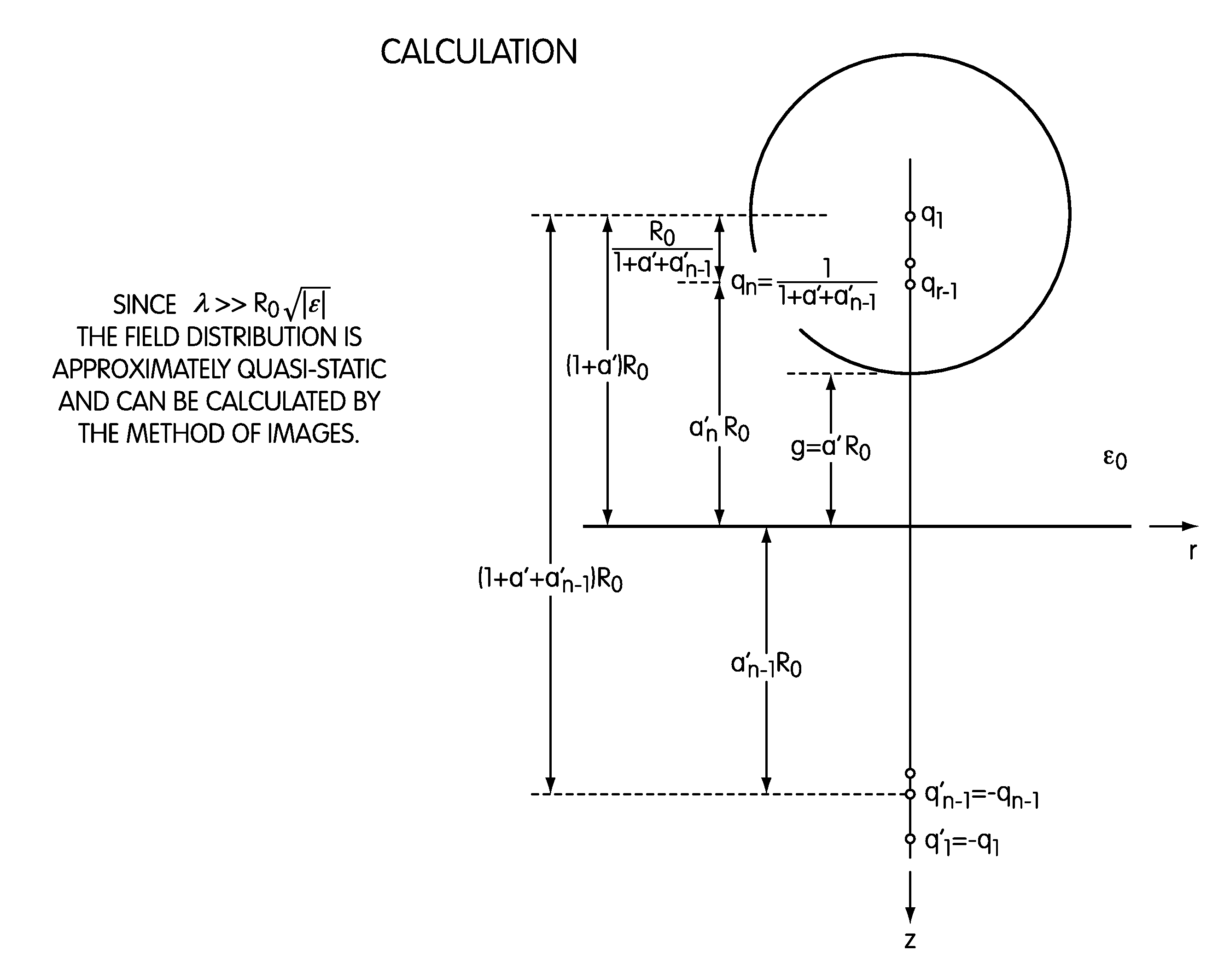
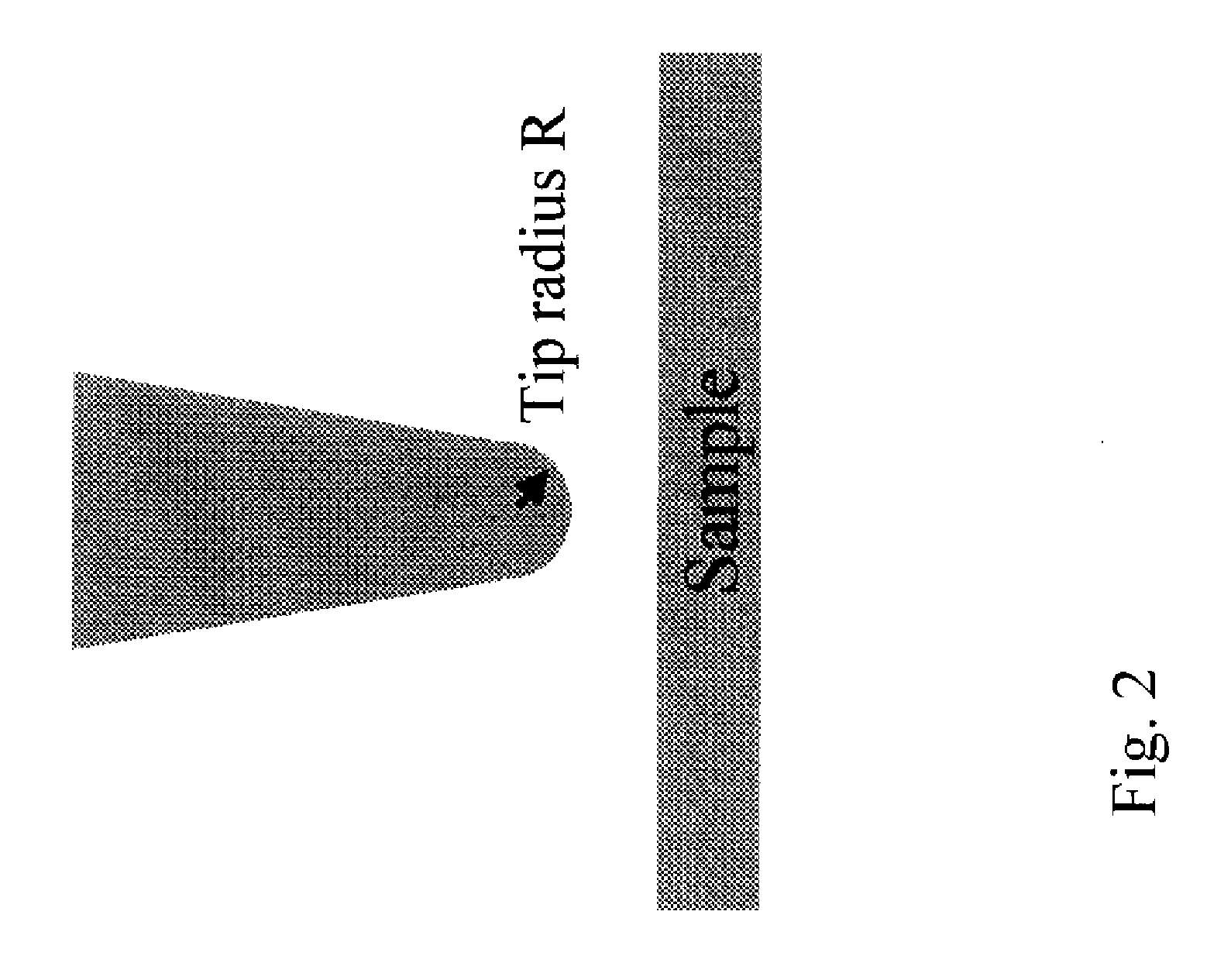
[0034]To determine quantitatively the physical properties, such as the complex dielectric constant, nonlinear dielectric constant and conductivity, through measurements of changes in resonant frequency (fr) and quality factor (Q) as function of different materials, bias electric and magnetic fields, tip-sample distance and temperature, etc. by a scanned evanescent microwave probe (SEMP), a quantitative model of the electric and magnetic fields in the tip-sample interaction region is necessary. A number of quasistatic models can be applied to the calculation of the probe response to dielectric, nonlinear dielectric and conductive materials. For the present invention, these models are applied to the calculation of the complex dielectric constant, nonlinear dielectric constant, and conductivity.
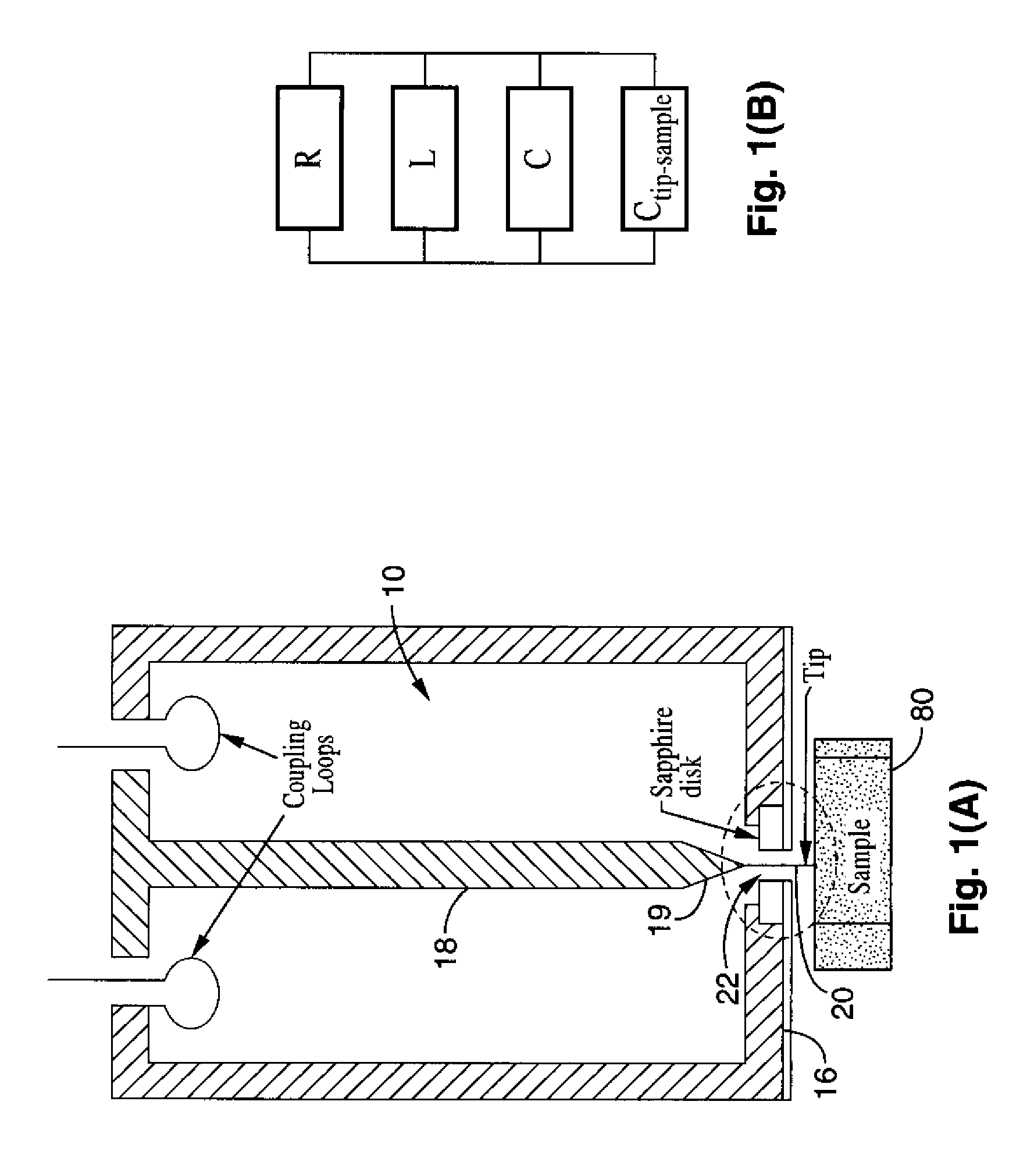
[0035]To determine the electrical properties of a sample, the variation in resonant frequency (fr) and quality factor (Q) of a resonant cavity is measured. (FIG. 1(A)). The tip-sample interactio...
embodiment b
[0084]The above described models are applied to the regulation of the tip-sample separation for dielectric and conductive materials. In principle, with above models, the relationship between tip sample distance, electrical impedance and measured signals (fr and Q as function of sample difference, bias fields and other variables) is known precisely, at least when the tip is very close to the sample. If measured fr and Q signal points (and their derivatives with respect to electric or magnetic fields, distance and other variables) are more than unknown parameters, the unknowns can be uniquely solved. If both tip-sample distance and electrical impedance can be determined simultaneously, then the tip-sample distance can be easily controlled, so that the tip is always kept above the sample surface with a desired gap (from zero to microns). Both topographic and electrical impedance profiles can be obtained. The calculation can be easily performed by digital signal processor or any compute...
embodiment c
[0109]By contrast to most types of microscope, SEMM measures a complex quantity, i.e., the real and imaginary parts of the electrical impedance. This is realized by measuring the changes in the resonant frequency (fr) and quality factor (Q) of the resonator simultaneously. A conventional method of measuring these two quantities is to sweep the frequency of the microwave generator and measure the entire resonant curve. For each measurement, this can take seconds to minutes depending on the capabilities of the microwave generator. These measurements are limited by the switching speed of a typical microwave generator to roughly 20 Hz. With the use of a fast direct digital synthesizer based microwave source, the throughput can be improved to roughly 10 kHz, but is still limited by the need to switch over a range of frequencies. Another method is to implement an analog phase-locked loop for frequency feedback control. This method can track the changing resonant frequency in real time and...
PUM
| Property | Measurement | Unit |
|---|---|---|
| wavelength | aaaaa | aaaaa |
| wavelength | aaaaa | aaaaa |
| distance | aaaaa | aaaaa |
Abstract
Description
Claims
Application Information