Joint optimisation of supply and bias modulation

a bias modulation and supply optimization technology, applied in the field of amplification of radio frequency (rf) signals, can solve problems such as limiting the usefulness of a dual bias architecture, and achieve the effect of optimizing system performance objectives

Inactive Publication Date: 2009-12-10
SNAPTRACK
View PDF0 Cites 60 Cited by
  • Summary
  • Abstract
  • Description
  • Claims
  • Application Information

AI Technical Summary

Benefits of technology

[0028]Feedback from the output of said RF amplifier may be used to assist updating of said non-linear mapping functions. The non-linear supply mapping means and said non-linear bias mapping means may be updated in accordance with the temperature of said RF amplification stage. Pre

Problems solved by technology

Without the solution provided by the invention, the complex and interdependent nature of key amplifier performance parameters (pa

Method used


Image

  • Joint optimisation of supply and bias modulation
  • Joint optimisation of supply and bias modulation
  • Joint optimisation of supply and bias modulation

Examples


first embodiment

[0082]An arrangement in accordance with the invention is now described with reference to FIG. 14. Elements of this Figure which correspond to elements shown in FIG. 1 are identified by like reference numerals. FIG. 14 illustrates an embodiment in which the invention is implemented in the analogue domain.

[0083]In the embodiments of FIG. 14, and subsequent embodiments described herein, there is shown an amplification stage 100 comprising a single RF amplifier. It should be understood, as discussed hereinabove, that the invention is not limited to any specific amplifier arrangement.

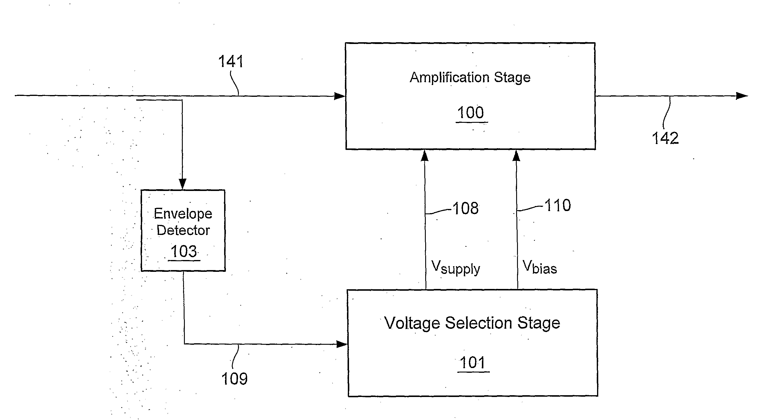
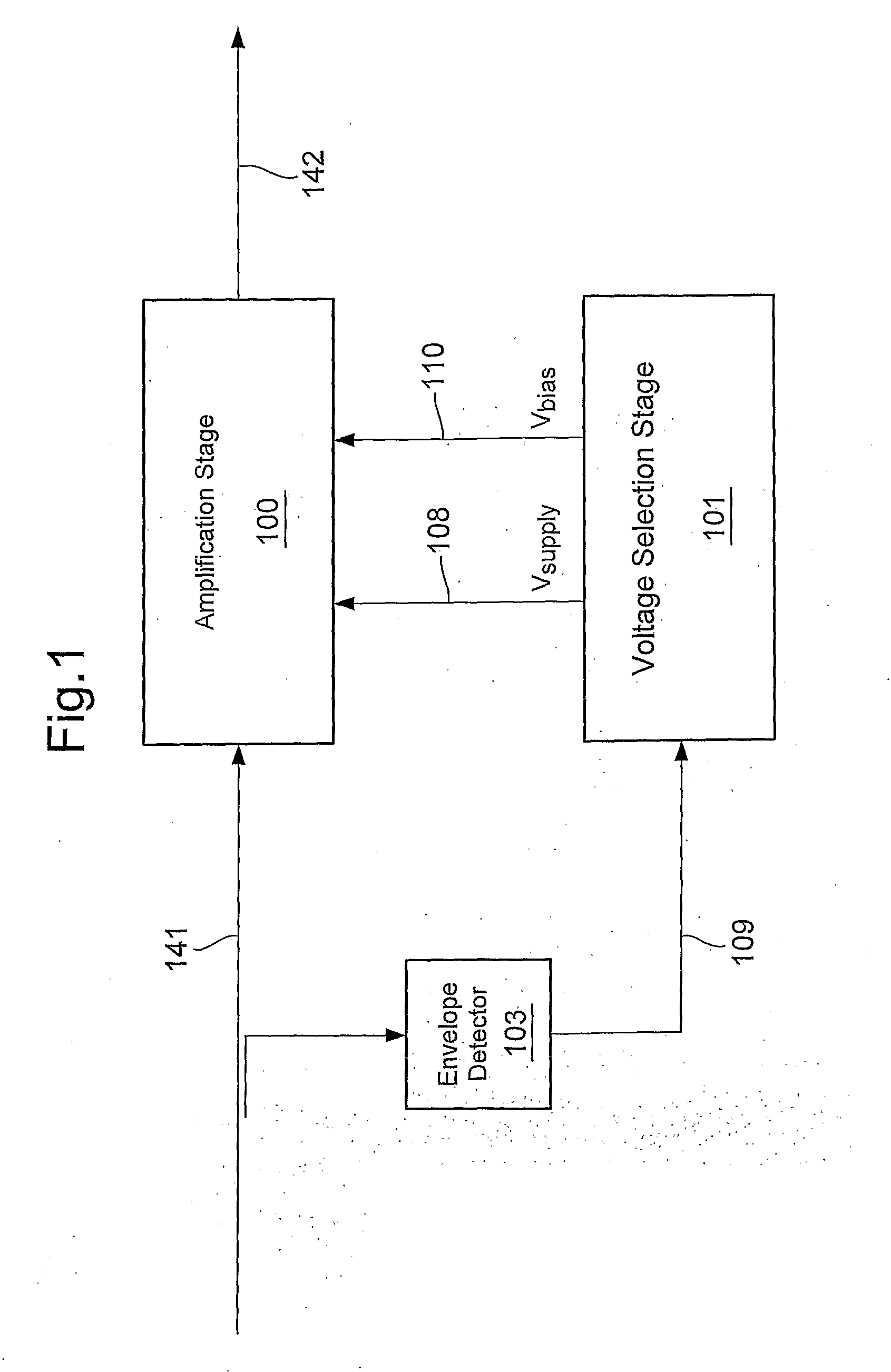
[0084]In the arrangement of FIG. 14 the amplifier 100 receives an RF input signal at a first input port on line 141, a continuously variable amplifier supply voltage on a line 108 at a second input port, and an amplifier bias voltage on line 110 at a third input port. The amplifier generates an RF output signal on line 142 at an output port.

[0085]The RF amplifier is fed with a non-constant envelope signal (e...

second embodiment

[0091]An arrangement in accordance with the invention is now described with reference to FIG. 15. Elements of this Figure which correspond to elements shown in FIGS. 1 and 13 are identified by like reference numerals. FIG. 15 illustrates an embodiment in which the invention is illustrated in the digital domain.

[0092]In this embodiment, envelope detection is performed in the digital domain. Similarly, the non-linear mappings for supply and bias voltages are also carried out in the digital baseband. One advantage of this embodiment is the ease of implementing delay elements in the digital domain, which males it easier to obtain precise time alignment between the RF envelope input signal and the amplifier supply and bias voltages.

[0093]The amplifier supply voltage on line 109 provided by the output of the DC-DC converter 102 on line 109. The DC-DC converter 102 is controlled by an output on line 112 from a non-linear mapping entity 116. The amplifier bias voltage on line 110 is provide...

third embodiment

[0098]In practice, the implementation of any embodiment in accordance with the invention will be in either the analogue domain as illustrated by the example of FIG. 14, or the digital domain as illustrated by the example of FIG. 15. However in a third embodiment, as illustrated by FIG. 16, the analogue and digital arrangements may be provided in parallel. Elements of this Figure which correspond to elements shown in any previous Figure are identified by like reference numerals. FIG. 16 illustrates an arrangement in which the invention is implemented in either the analogue or digital domain.

[0099]For the purpose of illustration in FIG. 16 a switch 112 is shown which selects between the Output of the non-linear digital mapping element 116 or the output of the non-linear analogue mapping element 104, and provides the selected output to the DC-DC converter 102. Similarly a switch 114 is provided which selects either the output of the non-linear digital mapping element 138 or the output ...


PUM


Abstract

A radio frequency amplifier system is disclosed in which the amplifier bias supply and power supply voltages are >instantaneously modulated with signals derived from the envelope voltage of the input signal. Separate non-linear mapping functions are used to derive the supply and bias voltages. The two mapping functions are optimised jointly to achieve particular system performance goals, such as optimum efficiency, constant gain, constant phase, or minimum spectral spreading. An optimisation of >particular interest is that which achieves best RF amplifier power added efficiency subject to achieving constant amplifier gain. In this way the need for pre-distortion linearization may be reduced or eliminated.

Description

FIELD OF THE INVENTION[0001]The invention relates to techniques for achieving amplification of non-constant envelope signals. The invention particularly, but not exclusively, relates to the amplification of radio frequency (RF) signals.DESCRIPTION OF THE RELATED ART[0002]Many modern communication systems typically use non-constant envelope modulation techniques to achieve high spectral efficiency. To avoid spectral spreading into adjacent communication channels, high linearity radio frequency (RF) amplification is required. Traditional fixed bias amplifiers can only achieve the required linearity by ‘backing off’ the amplifier so that it normally operates at a power well below its peak power capability. Unfortunately, the DC to RF power conversion efficiency in this region is very low. As a consequence these designs dissipate considerable heat and reduce battery life when used in portable applications.[0003]Maximisation of battery life is of paramount importance in mobile wireless e...

Claims


Application Information

Patent Timeline
IPC IPC(8): H03F1/02
CPCH03F1/0227H03F2200/451H03F2200/102H03F1/3241
Inventor WIMPENNY, GERARD
Owner SNAPTRACK
Why Eureka
Try Eureka