Compact multi-port cam cell implemented in 3D vertical integration

a multi-port, cam cell technology, applied in the field of semiconductor devices, can solve the problems of reducing the performance of the microprocessor, adding latency, and preventing requests from being granted access, and achieve the effect of substantially reducing the negative effect of increasing the travel distan

Inactive Publication Date: 2009-12-10
GLOBALFOUNDRIES INC
View PDF15 Cites 8 Cited by
  • Summary
  • Abstract
  • Description
  • Claims
  • Application Information

AI Technical Summary

Benefits of technology

[0013]The present invention provides a multi-ported CAM cell in which the negative effects of increased travel distance have been substantially reduced. This is achieved in the present invention by utilizing three-dimensional integration in which multiple active circuit layers are vertically stacked and vertically aligned interconnects are employed to connect a device from one of the stacked layers to another device in another stacked layer.
[0014]By vertically stacking multiple active circuit layers with vertically aligned interconnects, each compare port of a multi-port CAM can be implemented on a separate layer above or below the primary data storage cell. This allows the multi-port CAM structure to be implemented within the same area footprint as a standard Random Access Memory (RAM) cell, minimizing data access and match compare delays. Each compare match line and data bit line has the length associated with a simple two-dimensional Static Random Access Memory (SRAM) cell array.
[0015]The inventive three-dimensional approach allows the interconnect delays of match lines and bit lines for a multi-port CAM to be comparable to those associated with the bit lines of a conventional two-dimensional RAM array. The match line access is improved over the standard 2D approach for single and multi-port CAM arrays. The base RAM layer can be identical to standard SRAM, eliminating the need for additional reticle enhancement techniques to be developed for a CAM cell.

Problems solved by technology

This means that when there are simultaneous requests among more than one of the requesters, that some requests are delayed from being granted access to the cache.
This delay reduces the performance of the microprocessor by adding latency to the “losing” operations.
This area increase would result in longer wire travel distances which would cause the access time to slow down.

Method used


Image

  • Compact multi-port cam cell implemented in 3D vertical integration
  • Compact multi-port cam cell implemented in 3D vertical integration
  • Compact multi-port cam cell implemented in 3D vertical integration

Examples


Embodiment Construction

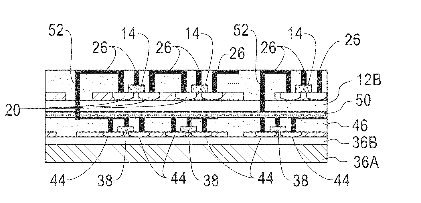
[0037]The present invention, which provides a compact multi-port CAM cell and a method of fabricating the same, will now be described in greater detail by referring to the following discussion and drawings that accompany the present application. It is noted that the drawings are provided for illustrative purposes only. As such, the drawings included within the present application are not drawn to scale.

[0038]In the following description, numerous specific details are set forth, such as particular structures, components, materials, dimensions, processing steps and techniques, in order to provide a thorough understanding of the present invention. However, it will be appreciated by one of ordinary skill in the art that the invention may be practiced without these specific details. In other instances, well-known structures or processing steps have not been described in detail in order to avoid obscuring the invention.

[0039]It will be understood that when an element as a layer, region or...


PUM


Abstract

A multi-ported CAM cell in which the negative effects of increased travel distance have been substantially reduced is provided. The multi-ported CAM cell is achieved in the present invention by utilizing three-dimensional integration in which multiple active circuit layers are vertically stack and vertically aligned interconnects are employed to connect a device from one of the stacked layers to another device in another stack layer. By vertically stacking multiple active circuit layers with vertically aligned interconnects, each compare port of the multi-port CAM can be implemented on a separate layer above or below the primary data storage cell. This allows the multi-port CAM structure to be implemented within the same area footprint as a standard Random Access Memory (RAM) cell, minimizing data access and match compare delays. Each compare match line and data bit line has the length associated with a simple two-dimensional Static Random Access Memory (SRAM) cell array.

Description

CROSS-REFERENCE TO RELATED APPLICATIONS[0001]This application is a divisional of U.S. Ser. No. 11 / 750,631, filed May 18, 2007, the entire contents of which are incorporated herein by reference.BACKGROUND[0002]The present invention relates to a semiconductor structure and a method of fabricating the same. More particularly, the present invention relates to a multi-port Content Addressable Memory (CAM) cell in which each compare port of the CAM cell is located in a separate layer vertically abutting the primary data storage cell. The present invention also provides a method of forming such a multi-ported CAM cell in which three-dimensional (3D) integration is employed in forming the same.[0003]Nearly every modem microprocessor employs a cache whereby some instructions and / or data are kept in storage that is physically closer and more quickly accessible than from the main memory. This type of storage is commonly known as a cache. When the cache is tightly integrated into the processor'...

Claims


Application Information

Patent Timeline
Patent Type & Authority Applications(United States)
IPC IPC(8): H01L21/00H01L21/46
CPCG11C15/00H01L21/6835H01L2924/1306H01L24/24H01L24/82H01L25/0657H01L25/50H01L27/0688H01L27/1203H01L2221/68368H01L2224/24226H01L2224/83894H01L2225/06513H01L2225/06541H01L2924/01004H01L2924/01013H01L2924/01029H01L2924/01033H01L2924/01074H01L2924/04953H01L2924/10329H01L2924/14H01L2924/19041H01L2924/19043H01L2924/30105H01L2924/01005H01L2924/01006H01L2924/00H01L2224/80896H01L2224/9202H01L2224/9212H01L2224/8203H01L2224/821H01L2224/80001H01L2224/82
Inventor BUCKI, ROBERT J.ATWAL, JAGREET S.BARNES, JOSEPH S.BERNSTEIN, KERRYROBINSON, ERIC
Owner GLOBALFOUNDRIES INC
Why Eureka
Try Eureka