Liquid crystalline organic semiconductor material and organic electron device

a technology of organic semiconductors and semiconductor materials, which is applied in the direction of naphthalimide/phthalimide dyes, non-metal conductors, anthracene dyes, etc., can solve the problems of low orientation/alignment order of molecule orientation/alignment, and the conventional electronic devices using inorganic semiconductor materials such as silicon do not meet the requirements

Active Publication Date: 2009-12-24
FUJIFILM CORP
View PDF4 Cites 20 Cited by
  • Summary
  • Abstract
  • Description
  • Claims
  • Application Information

AI Technical Summary

Benefits of technology

[0012]Other and further features and advantages of the invention will appear more fully from the following description, appropriately referring to the accompanying drawings.

Problems solved by technology

For such a terminal, a flexible, light-weight, and inexpensive electronic device is required, but conventional electronic devices using an inorganic semiconductor material such as silicon do not sufficiently meet the requirement.
However, the orientation / alignment order of the molecule is low.

Method used


Image

  • Liquid crystalline organic semiconductor material and organic electron device
  • Liquid crystalline organic semiconductor material and organic electron device
  • Liquid crystalline organic semiconductor material and organic electron device

Examples


example 1

(Liquid Crystallinity)

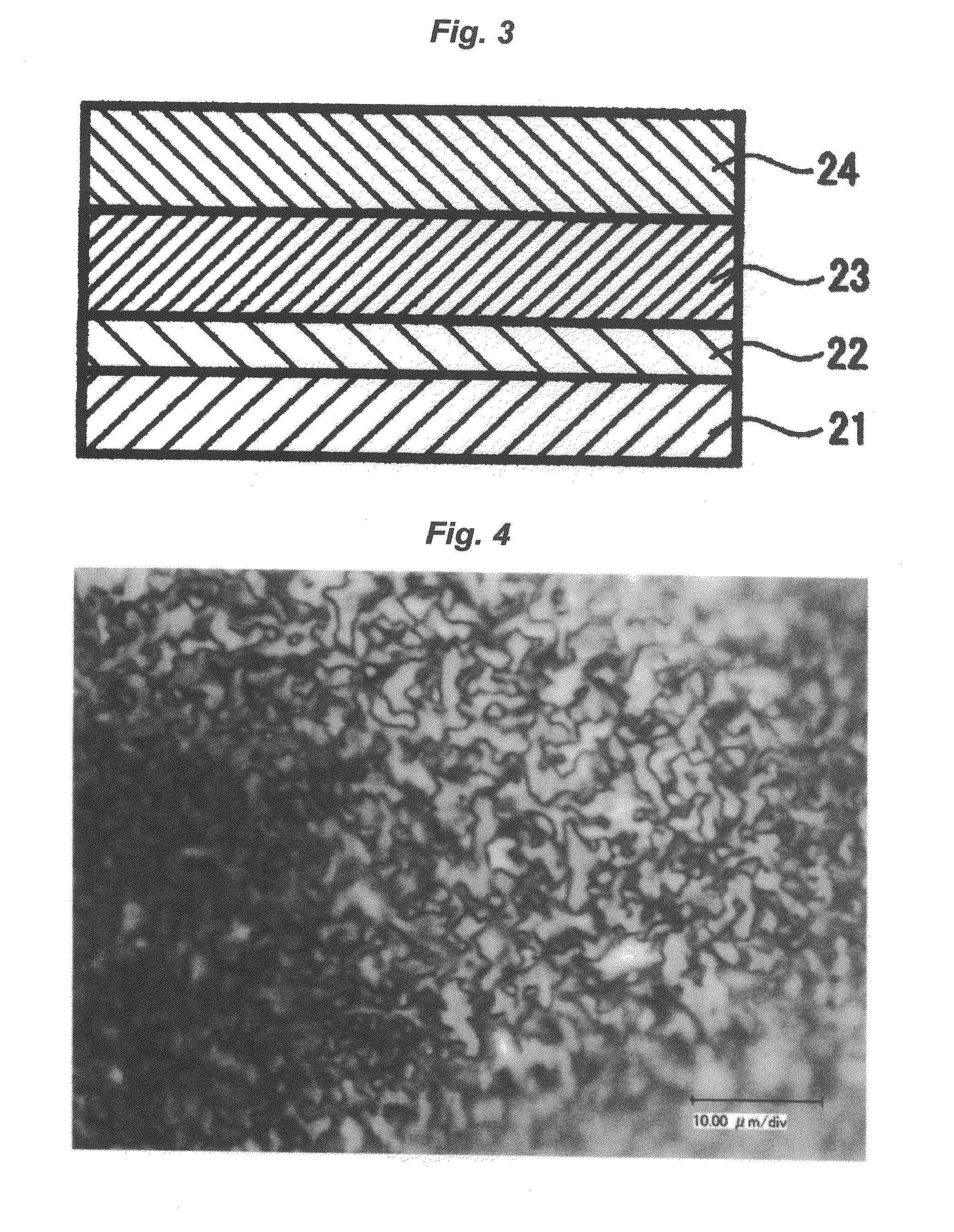
[0179]The exemplified compound 2 was heated to 300° C. on a quartz substrate, and then cooled to room temperature. A polarizing microscope was used to observe the compound under a cross nicol condition. As a result, a texture as shown in FIG. 4 was observed. From this fact, it was ascertained that the exemplified compound 2 exhibited liquid crystallinity at room temperature.

[0180]The exemplified compound 2 was measured by DSC and observed with the polarizing microscope. As a result, it was observed that the compound was changed from a liquid crystal phase to an isotropic liquid crystal phase at about 252° C. when the compound was heated.

example 2

(Characteristic of Organic Thin-Film Transistor)

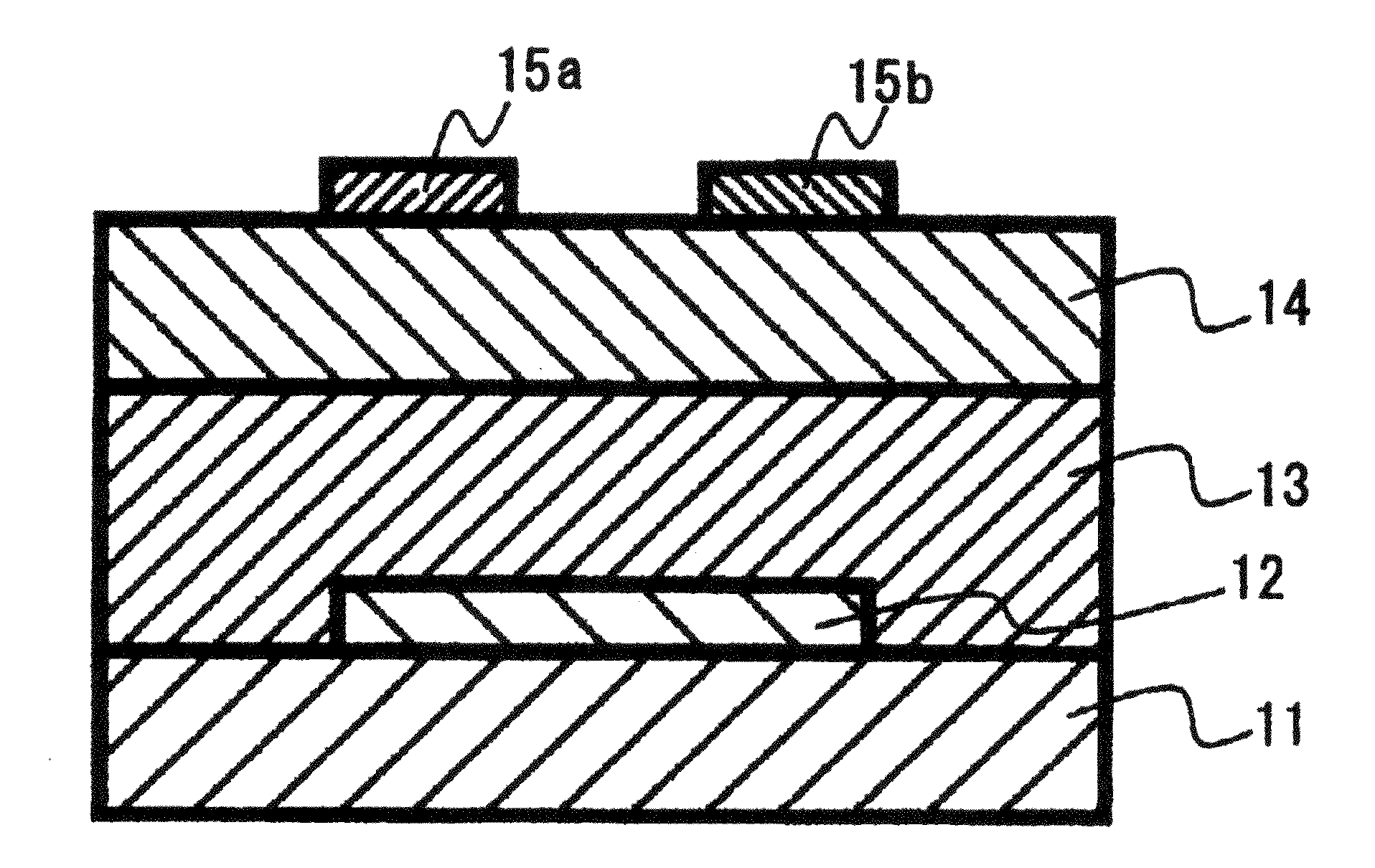
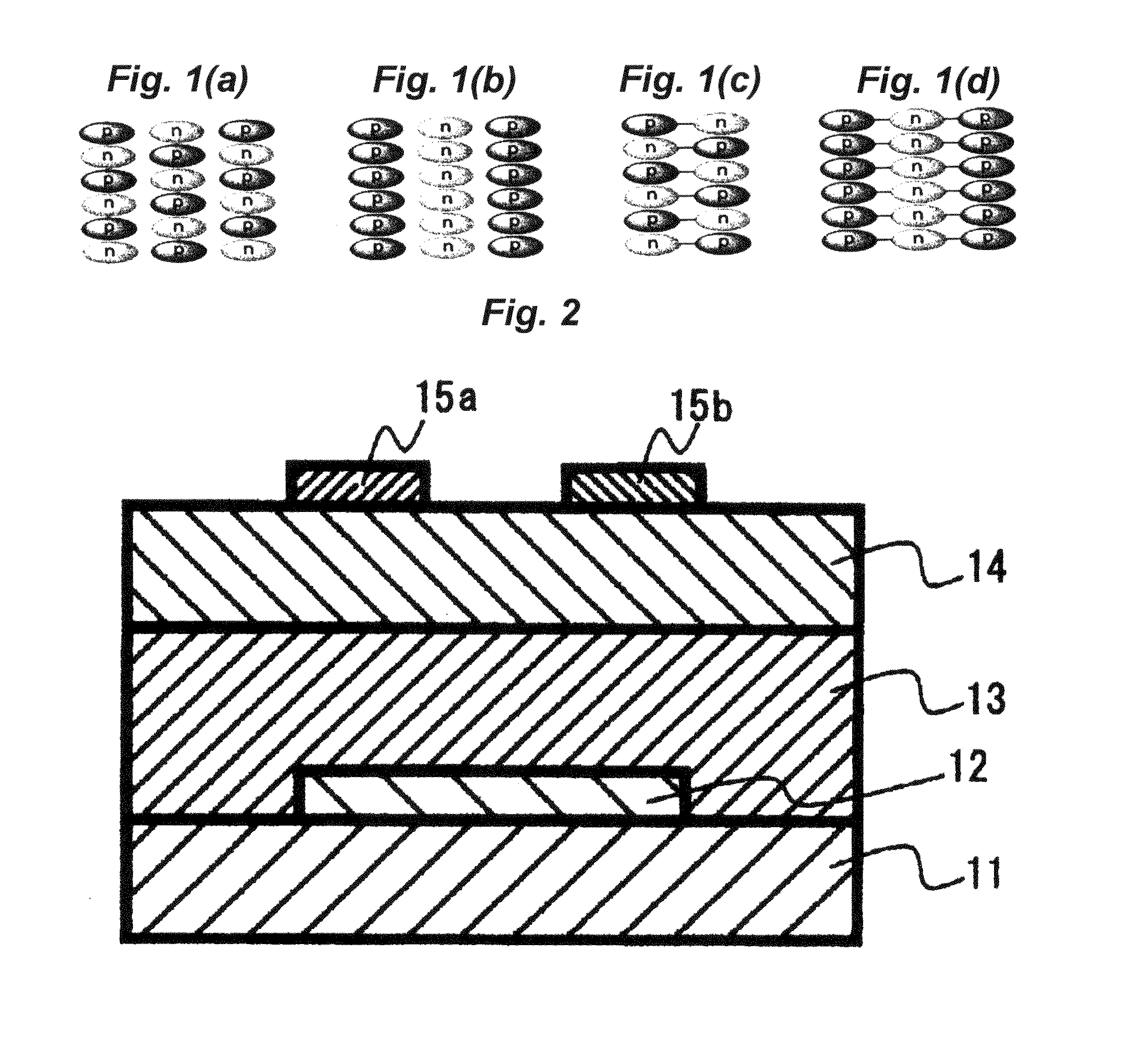
[0182]The exemplified compound 2 (1 mg) was dissolved into chloroform (1 mL), and the solution was drop-cast onto a FET-property-measuring substrate to yield a FET-property-measuring sample having an even thickness of 500 nm or less. The used FET-property-measuring substrate was a bottom-contact type substrate (its source and drain electrodes were each made of chromium / gold arranged in a comb form (gate width W=100000 μm, and gate length L=100 μm)) illustrated schematically in FIG. 5; its insulator film was made of SiO2 (film thickness: 200 nm); and its substrate was made of silicon). The FET characteristic was measured with a semiconductor parameter analyzer (trade name: 4156C, manufactured by Agilent Co,) to which a semiautomatic prober (trade name: AX-2000, manufactured by Vector Semiconductor Co., Ltd.) was connected, under normal pressure in a nitrogen atmosphere (in a glove box). A result of the examination or observation of the ...

example 3

(Characteristic of Organic Thin-Film Photoelectric Conversion Device)

[0184]A glass substrate (2.5 cm×2.5 cm) having thereon a patterned ITO electrode was washed with ultrasonic waves in isopropyl alcohol, and then dried. Furthermore, in order to remove any organic pollutants on the ITO electrode surface, the substrate was treated with UV ozone for 30 minutes. Next, the ITO substrate was spin-coated (at 4000 rpm for 60 seconds) with a solution of PEDOT (poly(3,4-ethylenedioxythiophene)) / PSS (polystyrenesulfonic acid) in water (Baytron P (standard product)), and then the whole was dried at 120° C. for 10 minutes to form a hole-transporting buffer layer having a film thickness of about 50 nm. The film thickness was measured with a probe-used thickness meter (trade name: DEKTAK 6M, manufactured by ULVAC, Inc.) [the same matter will be correspondingly applied to the following description]. Next, a 1.0 mg / mL solution of the exemplified compound 2 in chloroform was drop-cast onto the buffe...


PUM

PropertyMeasurementUnit
phase transition temperatureaaaaaaaaaa
thicknessaaaaaaaaaa
thicknessaaaaaaaaaa

Abstract

A liquid crystalline organic semiconductor material, having a compound having at least one bonding form selected from the group consisting of (p-type organic semiconductor compound residue)-(n-type organic semiconductor compound residue)-(p-type organic semiconductor compound residue), and (n-type organic semiconductor compound residue)-(p-type organic semiconductor compound residue)-(n-type organic semiconductor compound residue).

Description

FIELD OF THE INVENTION[0001]The present invention relates to a novel liquid crystalline organic semiconductor material, a thin film containing the liquid crystalline organic semiconductor material, and an organic electronic device (in particular, an organic thin-film transistor or an organic thin-film photoelectric conversion device) using the liquid crystalline organic semiconductor material.BACKGROUND OF THE INVENTION[0002]With the arrival of a ubiquitous information society, information terminals need to be able to transfer information anytime, anywhere. For such a terminal, a flexible, light-weight, and inexpensive electronic device is required, but conventional electronic devices using an inorganic semiconductor material such as silicon do not sufficiently meet the requirement. Accordingly, in recent years, electronic devices using organic semiconductor materials have been intensively studied for satisfying such requirements (Chemical Reviews, 2007, 107, 1296 to 1323 and “Organ...

Claims


Application Information

Patent Timeline
Patent Type & Authority Applications(United States)
IPC IPC(8): H01L51/54H01B1/12C07D471/04
CPCC07D471/06Y02E10/549C09K19/3488C09K19/3491C09K19/3497C09K19/40C09K2019/0496H01L51/0053H01L51/006H01L51/0061H01L51/0068H01L51/0076H01L51/0095H01L51/4206H01L51/4253C09K19/3483C09B5/62C09B57/007C09B57/08H10K85/621H10K85/636H10K85/633H10K85/655H10K85/731H10K85/791H10K30/451H10K30/30
Inventor KITAMURA, TETSU
Owner FUJIFILM CORP
Why Eureka
Try Eureka